

Optical transmitter and optical transmission system
a technology which is applied in the field of optical transmission system and optical transmitter, can solve the problems of difficult to limit the effect of waveform deterioration, difficult to satisfy, and waveform deterioration, and achieve excellent transmission characteristics and excellent quality
- Summary
- Abstract
- Description
- Claims
- Application Information
AI Technical Summary
Benefits of technology
Problems solved by technology
Method used
Image

Examples
first embodiment
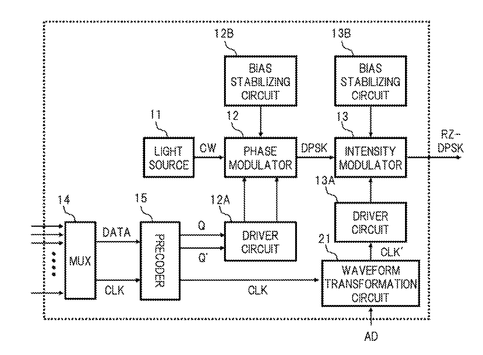
[0035]FIG. 1 is a block diagram showing the structure of an optical transmitter according to the present invention.
[0036]In FIG. 1, the present optical transmitter is provided for example with a waveform transformation circuit 21 in the conventional RZ-DPSK optical transmitter as shown in FIG. 11, that transforms the waveform of a clock signal CLK supplied from a precoder 15 to a driver circuit 13A that is associated with an intensity modulator 13 in which pulse carving is performed. A clock signal CLK′ whose duty cycle is adjusted by the waveform transformation circuit 21 is input to the driver circuit 13A. The structure other than the point concerning the provision of the waveform transformation circuit 21, is basically the same as the conventional structure shown in FIG. 11.
[0037]To be specific, a light source 11 generates a continuous light CW having a required wavelength and optical power using for example a tunable laser diode or the like, and outputs the continuous light CW t...
second embodiment
[0051]Next is a description of the present invention.
[0052]FIG. 7 is a block diagram showing the structure of an optical transmitter according to the second embodiment of the present invention.
[0053]In FIG. 7, in the present optical transmitter, a bias shift circuit 22 for offsetting the operating point of the intensity modulator 13 that performs pulse carving by a predetermined amount in a preset direction is provided in the structure of the conventional RZ-DPSK optical transmitter shown for example in FIG. 11. The structure of the present embodiment differs from the case of the first embodiment in the point that the bias shift circuit 22 is provided instead of the waveform transformation circuit 21 in the structure of the first embodiment. The other structure is similar to the case of the first embodiment. Therefore, a specific description will be given here focusing on the structure and operation of the bias shift circuit 22.
[0054]In the first embodiment described previously, the...
PUM
| Property | Measurement | Unit |
|---|---|---|
| threshold voltage | aaaaa | aaaaa |
| photoelectric response | aaaaa | aaaaa |
| frequency | aaaaa | aaaaa |
Abstract
Description
Claims
Application Information