Active touch system

a technology of active touch and touch screen, applied in the field of touch screen, can solve the problems of affecting the accuracy of touch screen positioning, so as to improve the accuracy of positioning touch position, the judgment procedure after detection is greatly simplified, and the detection is faster and more reliable.

Active Publication Date: 2014-04-15
FOCALTECH ELECTRONICS SHENZHEN CO LTD
View PDF10 Cites 9 Cited by
  • Summary
  • Abstract
  • Description
  • Claims
  • Application Information

AI Technical Summary

Benefits of technology

[0042]Compared with the prior art, the present invention has the following beneficial effects.
[0043]In the present invention, active devices are introduced into a touch screen, so that sensing electroding units on the screen can respectively sense the touch of a touch object completely independently. The hardware sensing stage in the front end of the touch system is improved, the detection of the touched position is digitalized in space, so that the source of the touch signal achieves the precision up to each sensing electroding unit. According to magnitudes of signals of adjacent sensing electroding units or according to the distribution of signals in the area of sensing electroding units having touch signals, the precision of positioning a touched position can be improved so that even a fine position between adjacent sensing electroding units can be positioned.
[0044]By introducing active devices into the touch screen and improving the method of obtaining touch signals in the hardware sensing stage of the touch system, the judgment procedure after detection is greatly simplified, so that post-processing chip resources can be saved significantly, the detecting becomes quicker and more reliable, and the overall cost may be lower.
[0045]By introducing active devices into the touch screen, the sensing electroding units on the screen can operate completely independently, the judgment of multi-point touch is realized, and multi-point touch becomes easy and natural.

Problems solved by technology

However, due to the double-layer substrate structure of the resistive touch screen, when the touch screen and the display panel are laminated in use, the reflection of the touch screen may greatly affect the display performance such as brightness, contrast, and chroma, thus greatly degrading the display quality, and the increase of the backlight brightness of the display panel may cause higher power consumption.
The analog resistive touch screen has the problem of positioning drift, and needs calibration from time to time.
In addition, the electrode contact working mode of the resistive touch screen also reduces the service life of the touch screen.
However, the cost of the infrared touch screen and the ultrasonic touch screen is high, and the water drop and dust may impair the working reliability of the touch screen.
Particularly, due to their complicated structures and high power consumption, the infrared touch screen and the ultrasonic touch screen generally cannot be applied in portable products.
However, the planar capacitive touch screen also has the problem of positioning drift, and needs calibration from time to time.
The water drop may also impair the working reliability of the touch screen.
Particularly, due to its high power consumption and cost, the planar capacitive touch screen generally cannot be applied in portable products.
The distributed capacitance in the manufacturing and use environment may affect the working reliability of the touch screen, and the interference of the display driving signal and other electrical signals may influence the working of the touch screen, and the water drop may also impair the working reliability of the touch screen.
Therefore, the manufacturing process is complicated, and the cost is high, especially for the large-sized and even ultra large-sized touch screens.
Since each sensing line on a screen, no matter on a resistive touch screen or a capacitive touch screen, is directly connected to multiple sensing units, sensing units are not completely independent of each other.
In order to recognize multiple touch points, compared with single-point touch, the scanning mode of detection becomes more complicated and much time is spent on detection, or the judgment procedure after detection becomes complicated and requires strong computing power and large storage space and also consumes a lot of time.

Method used


Image

  • Active touch system
  • Active touch system
  • Active touch system

Examples


first embodiment

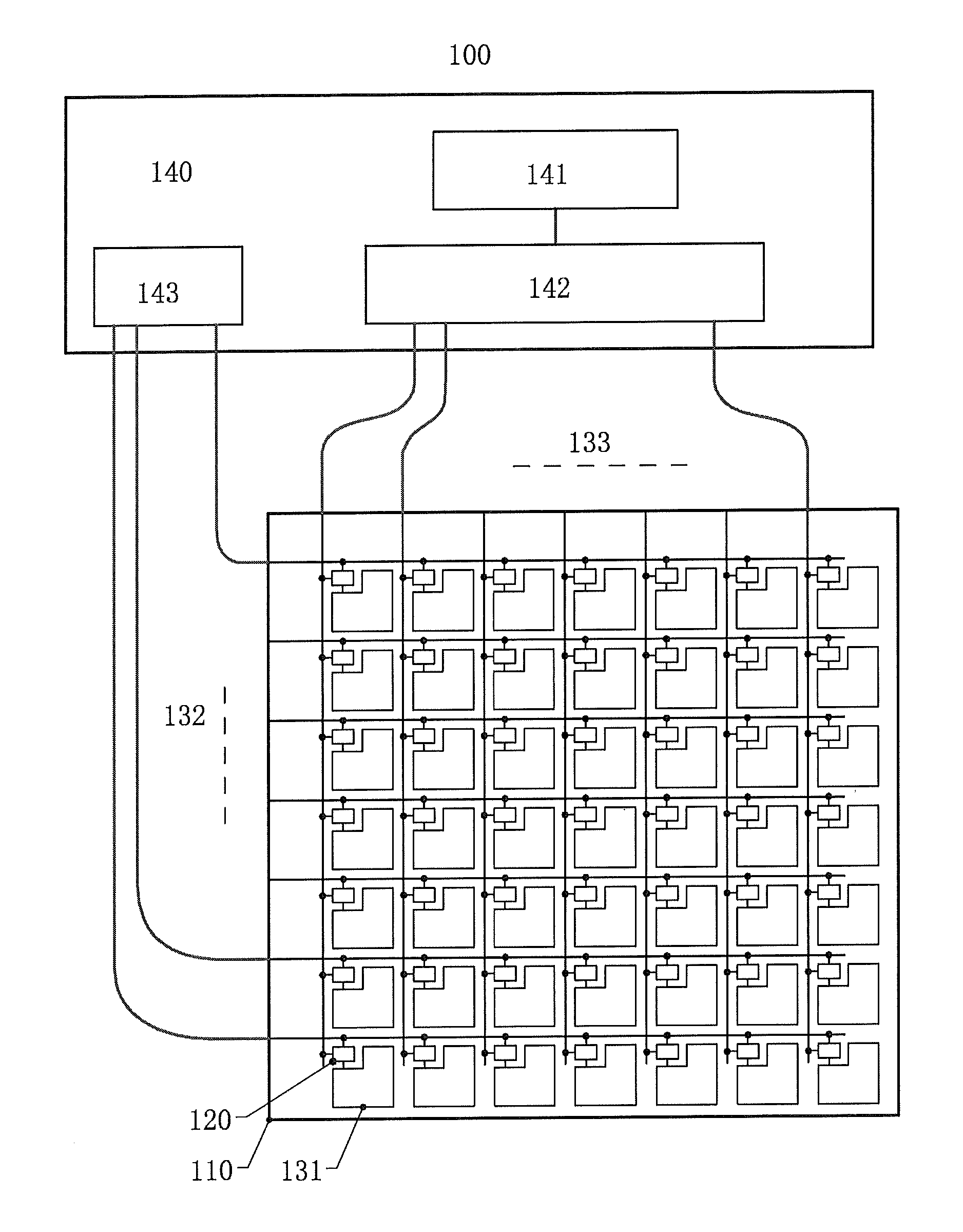
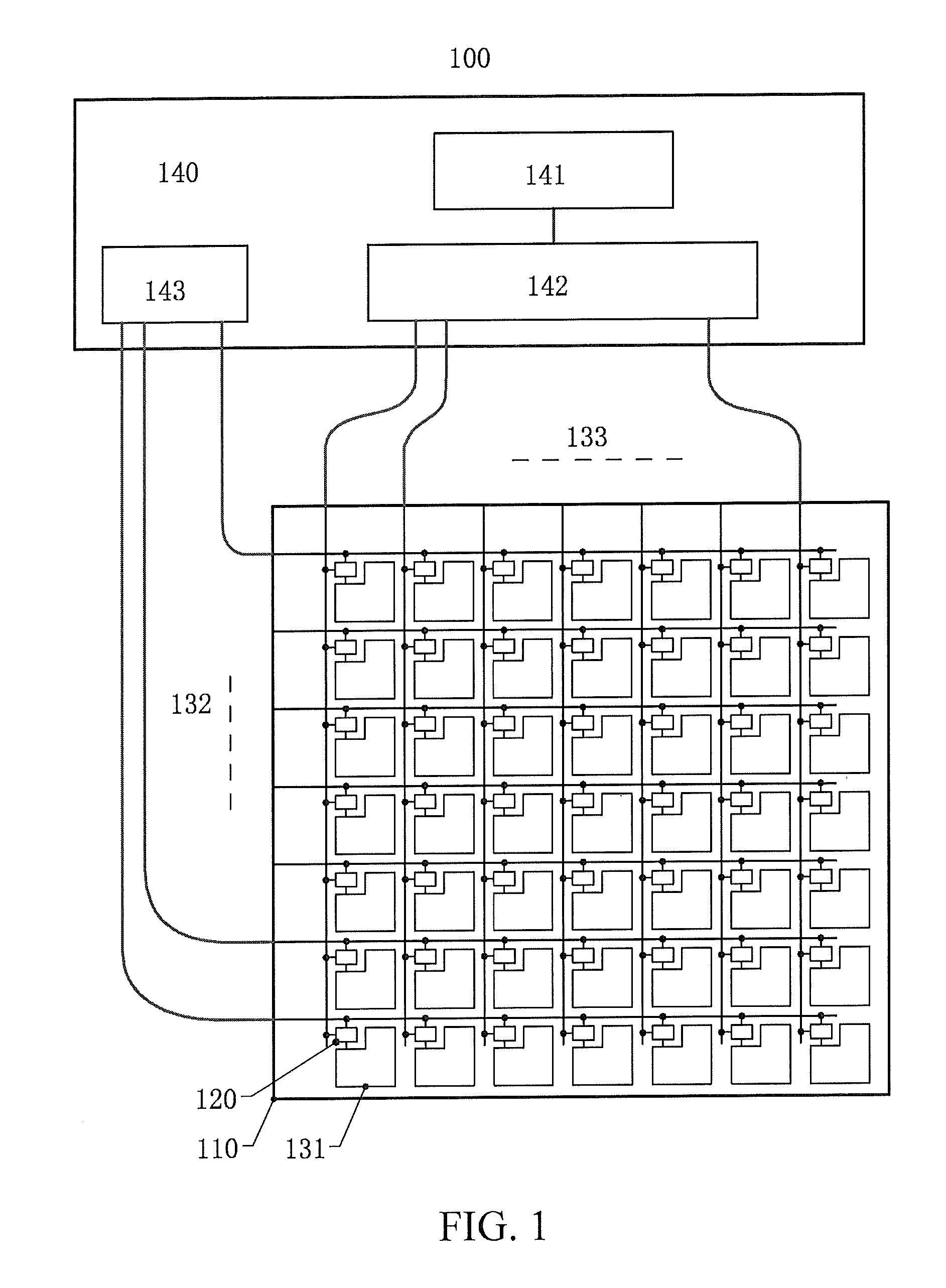
[0054]An active touch system 100 as shown in FIG. 1 includes a touch substrate 110, an active device array 120, sensing lines, and a touch system circuit 140. The three-terminal active device array 120 and the sensing line are disposed on the touch substrate 110. The sensing lines include a sensing electroding array 131 and two groups of intersecting row control electrodes 132 and column detecting lines 133. Each control electrode line and each detecting line are isolated by an insulating layer at an intersection thereof. The touch substrate 110 is a transparent substrate, each sensing electroding unit of the sensing electroding array 131 is a transparent indium tin oxide (ITO) electrode, the sensing electroding array 131, the row control electrodes 132, and the column detecting lines 133 are all disposed on a non-touch surface of the touch substrate 110 not facing users, and an insulating and protective outer layer is further disposed on the sensing electroding array 131, the row c...

second embodiment

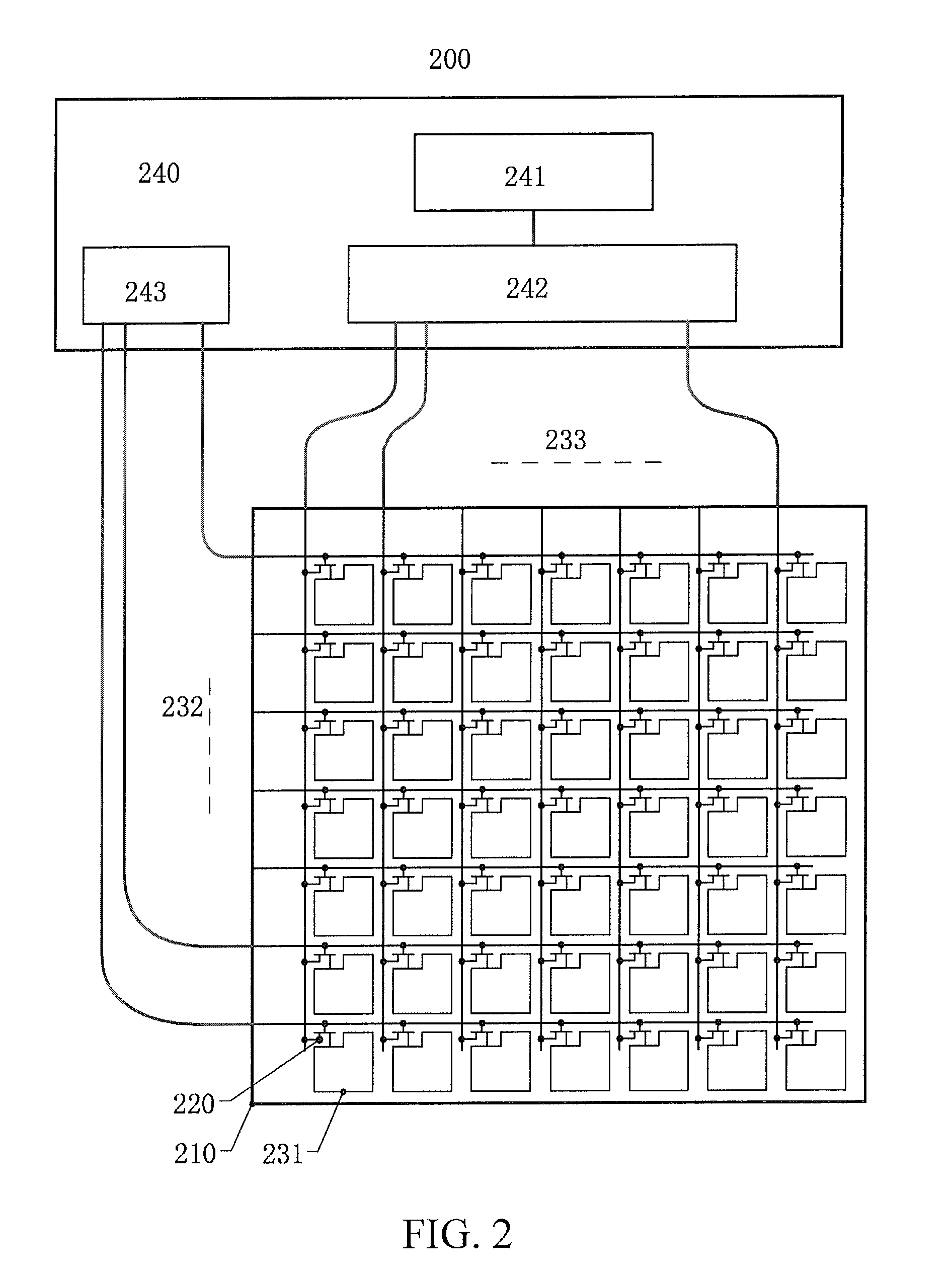
[0059]An active touch system 200 as shown in FIG. 2 includes a touch substrate 210, a thin film transistor (TFT) array 220, sensing lines, and a touch system circuit 240. The TFT array 220 and the sensing lines are disposed on the touch substrate 210. The sensing lines include a sensing electroding array 231 and two groups of intersecting row control electrodes 232 and column detecting lines 233, and each control electrode line and each detecting line are isolated by an insulating layer at an intersection thereof. The touch substrate 210 is a transparent substrate, each sensing electroding unit of the sensing electroding array 231 is a transparent ITO electrode, the sensing electroding array 231, the row control electrodes 232, and the column detecting lines 233 are all disposed on a touch surface of the touch substrate 210 facing users, and an insulating and protective outer layer is further disposed on the sensing electroding array 231, the row control electrodes 232, and the colu...

third embodiment

[0064]An active touch system 300 as shown in FIG. 3 includes a touch substrate 310, an active device array 320, sensing lines, and a touch system circuit 340. The two-terminal active device array 320 and the sensing lines are disposed on the touch substrate 310. The sensing lines include a sensing electroding array 331 and two groups of intersecting row control electrodes 332 and column detecting lines 333. Each control electrode line and each detecting line are isolated by an insulating layer at an intersection thereof. The touch substrate 310 is a flexible transparent substrate, each sensing electroding unit of the sensing electroding array 331 is a transparent ITO electrode, the sensing electroding array 331, the row control electrodes 332, and the column detecting lines 333 are all disposed on a non-touch surface of the touch substrate 310 not facing users. The touch system circuit 340 has a touch excitation source 341, a signal detection circuit 342, and a control circuit 343.

[...


PUM


Abstract

An active touch system is provided, in which sensing electroding units in an array and two groups of intersecting control electrodes and detecting lines are disposed on a touch substrate, and the detecting lines are connected to sensing electrodings through active devices. The control electrodes are used to control on and off of the active devices, and the detecting lines are used to apply touch excitation signals to the sensing electrodings, and detect a leakage current of a sensing electroding to a finger or other touch object. A position of the finger or other touch object on the touch substrate is found by determining a sensing electroding unit generating the leakage current. The method of obtaining touch signals is improved in the hardware sensing stage, so that the judgment procedure after detection is greatly simplified, and the judgment of multi-point touch becomes easy and natural.

Description

BACKGROUND OF THE INVENTION[0001]1. Field of the Invention[0002]The present invention relates to a touch screen, and more particularly to an active touch screen and a driving circuit thereof.[0003]2. Related Art[0004]Touch is the most important sensory perception of human beings, and is the most natural way in human-machine interaction. The touch screen thus emerges and has already been widely applied in personal computers, smart phones, public information, intelligent household appliances, industrial control, and other fields. In the current touch field, the resistive touch screen, photoelectric touch screen, ultrasonic touch screen, and planar capacitive touch screen are mainly developed, and in recently years, the projected capacitive touch screen is developed rapidly.[0005]So far, the resistive touch screen is still the mainstream product in the market. However, due to the double-layer substrate structure of the resistive touch screen, when the touch screen and the display panel...

Claims


Application Information

Patent Timeline
Patent Type & Authority Patents(United States)
IPC IPC(8): G06F3/041
CPCG06F3/0412G06F3/0416G06F3/044G06F2203/04104G06F2203/04107G06F3/04164G06F3/04166G06F3/0446G06F3/0443
Inventor CHEN, QILIANG
Owner FOCALTECH ELECTRONICS SHENZHEN CO LTD
Why Eureka
Try Eureka