High frequency power detector circuit and radio communication device

a detector circuit and high frequency technology, applied in the field of detector circuits, can solve problems such as errors in detected power levels and detection errors, and achieve the effects of improving resistance to variations, high frequency power, and raising the precision of high frequency power detection

Inactive Publication Date: 2014-05-27
PANASONIC CORP
View PDF9 Cites 0 Cited by
  • Summary
  • Abstract
  • Description
  • Claims
  • Application Information

AI Technical Summary

Benefits of technology

[0016]According to the configurations, an envelope of the high frequency signal is detected by the first envelope detector circuit, a reference voltage for power level detection is generated by the second envelope detector circuit of the same structure as the first envelope detector circuit, and an output of the first envelope detector circuit (an output of the selector or the variable gain amplifier, depending on the configuration) is detected by the detector with reference to an output of the second envelope detector circuit (an output of the selector or the variable gain amplifier, depending on the configuration). As a result, the power level of the input high frequency signal is detected. The first and second envelope detector circuits may be provided without using a current source. Further, there is no need of additionally providing a reference voltage generating circuit. Accordingly, the total number of resistive elements is kept small. Moreover, when the selector or the variable gain amplifier is accordingly controlled, it is possible to perform calibration and to detect multiple levels of power in a time-sharing manner. Therefore, as compared with conventional ones, the high frequency power detector circuit is improved in resistance against variations in the course of manufacture, change in temperature and change in supply voltage, thereby raising precision of high frequency power detection, and is reduced in size.
[0017]Preferably, the high frequency power detector circuit includes: a high frequency reference signal generating unit configured to generate a high frequency reference signal; an input selector configured to select either one of an actual high frequency signal or the high frequency reference signal, and input the selected signal to the level shifter; and a controller configured to control the input selector and the selector (the variable gain amplifier, depending on the configuration). The controller sequentially changes an output of the selector (a gain of the variable gain amplifier, depending on the configuration), during input of the high frequency reference signal to the level shifter, to store a control value for the selector (the variable gain amplifier, depending on the configuration) of the time when an output of the detector is inverted, and controls the selector (the variable gain amplifier, depending on the configuration) by using the stored control value when the actual high frequency signal is input to the level shifter. Specifically, the high frequency reference signal generating unit includes a local signal generator, an amplifier configured to clip an output of the local signal generator at an amplitude proportional to a power supply voltage, and an attenuator configured to attenuate an output of the amplifier. More specifically, the amplifier includes cascade-connected inverter circuits. With this configuration, calibrating the high frequency power detector circuit enables highly precise high-frequency power detection with small variations.

Problems solved by technology

Therefore, absolute values of a current and resistance vary due to variations in the course of manufacture, change in temperature and change in supply voltage, thereby causing an error in detected power level.
However, an error in detected power level may occur due to an error in input reference current and a mismatch between threshold values of paired transistors in the current mirror circuit.

Method used


Image

  • High frequency power detector circuit and radio communication device
  • High frequency power detector circuit and radio communication device
  • High frequency power detector circuit and radio communication device

Examples


first embodiment

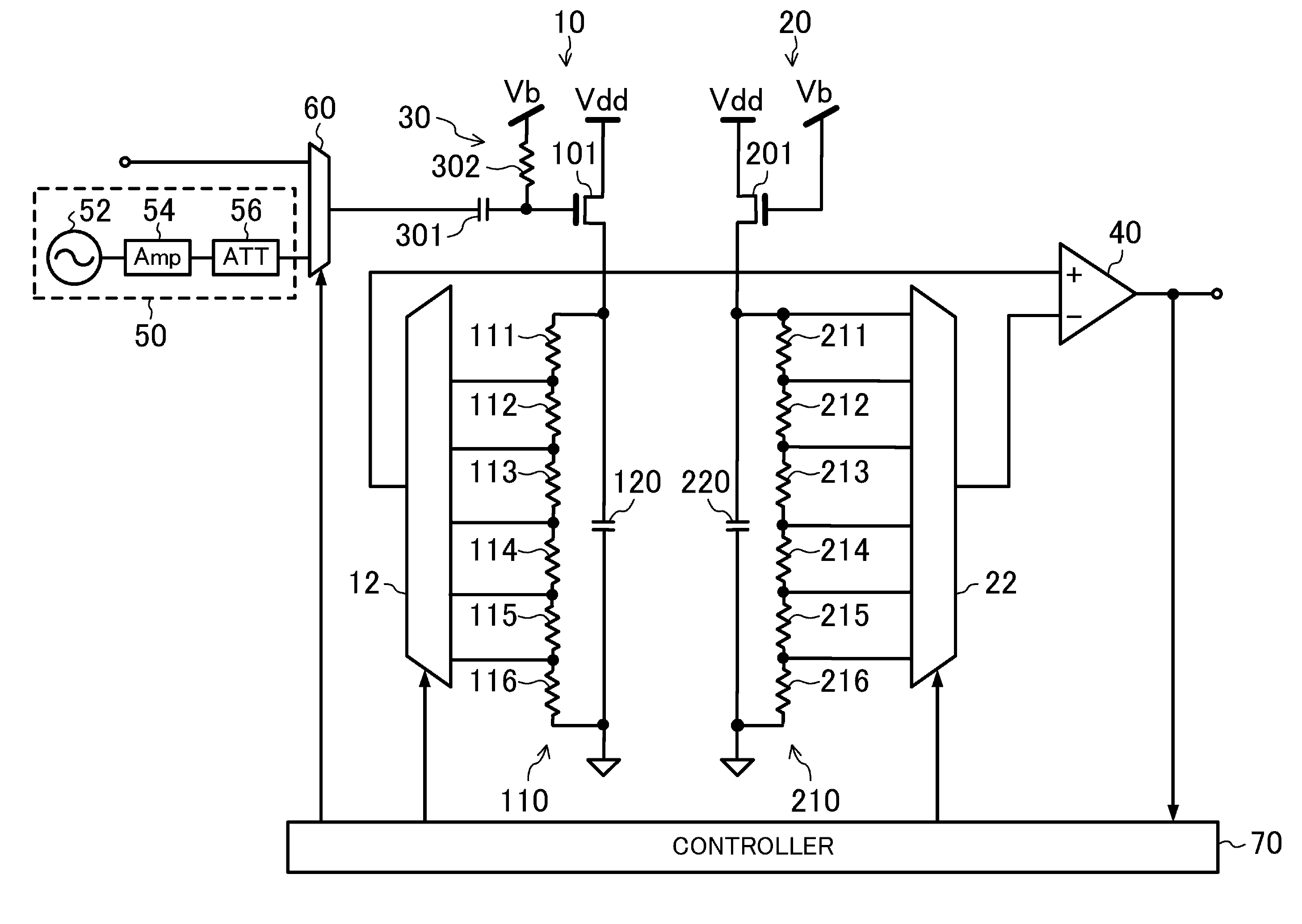
[0024]FIG. 1 shows the structure of a high frequency power detector circuit according to a first embodiment. In the envelope detector circuit 10, a drain of an N-channel field effect transistor 101 is connected to a supply voltage Vdd, and a resistance row 110 including six serially-connected resistive elements 111, 112, 113, 114, 115, and 116 and a capacitative element 120 are connected to a source of the transistor 101 in parallel. The structure of another envelope detector circuit 20 is the same as that of the envelope detector circuit 10. That is, in the envelope detector circuit 20, a drain of an N-channel field effect transistor 201 is connected to a supply voltage Vdd, and a resistance row 210 including six serially-connected resistive elements 211, 212, 213, 214, 215, and 216 and a capacitative element 220 are connected to a source of the transistor 201 in parallel. In the envelope detector circuits 10 and 20, corresponding elements have the same characteristic value. For ex...

second embodiment

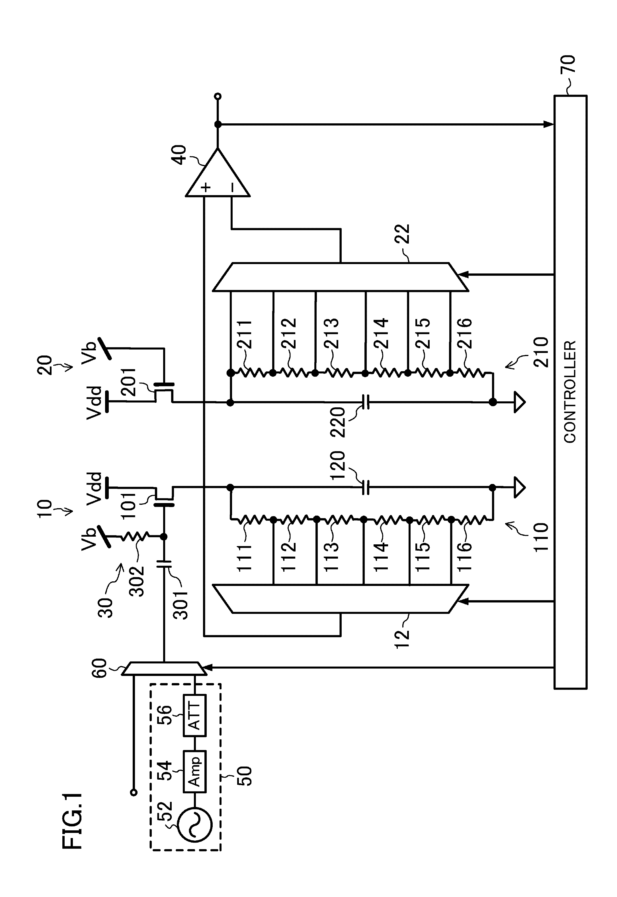
[0039]FIG. 2 shows the structure of a high frequency power detector circuit according to a second embodiment. The difference from the structure of the first embodiment is described below in detail. In the envelope detector circuit 10, a drain of an N-channel field effect transistor 101 is connected to a supply voltage Vdd, and a resistance row 110 including two serially-connected resistive elements 111 and 112 and a capacitative element 120 are connected to a source the transistor 101 in parallel. The structure of another envelope detector circuit 20 is the same as that of the envelope detector circuit 10. That is, in the envelope detector circuit 20, a drain of an N-channel field effect transistor 201 is connected to a supply voltage Vdd, and a resistance row 210 including two serially-connected resistive elements 211 and 212 and a capacitative element 220 are connected to a source of the transistor 201 in parallel. In the envelope detector circuits 10 and 20, corresponding element...

third embodiment

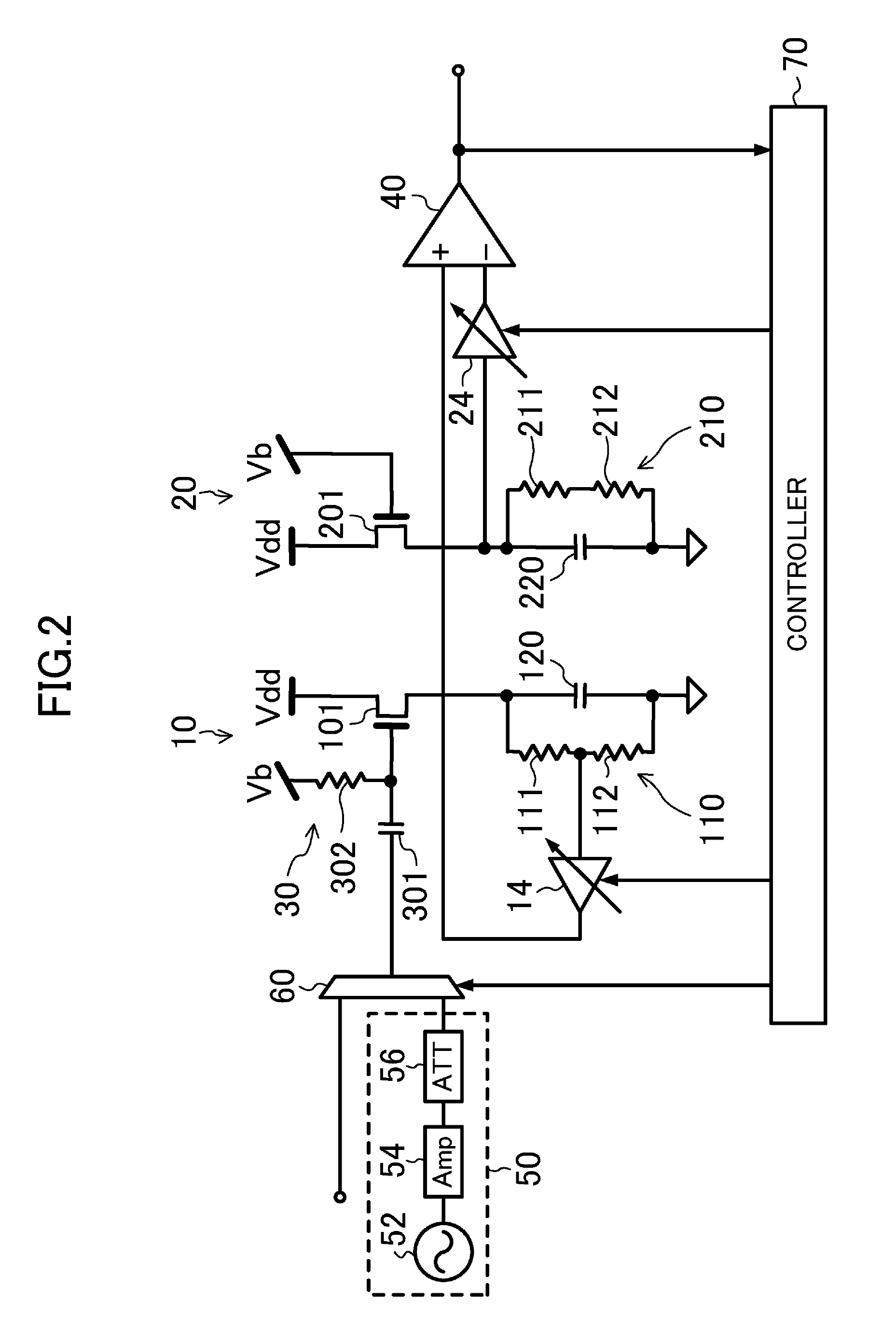
[0045]FIG. 3 shows the structure of a high frequency power detector circuit according to a third embodiment. The high frequency power detector circuit of the present embodiment is the high frequency power detector circuit of FIG. 1 in which the selector 12 is omitted, and a variable gain amplifier 16 is provided between the input selector 60 and the level shifter 30. The difference from the structure of the first embodiment is described below in detail.

[0046]The detector 40 detects an intermediate terminal voltage of the resistance row 110 of the envelope detector circuit 10 with reference to an output voltage of the selector 22. Although a voltage at a connection point of the resistive element 115 and the resistive element 116 is detected here, another intermediate terminal voltage may be detected.

[0047]The controller 70 controls the variable gain amplifier 16, the selector 22, and the input selector 60 to calibrate the high frequency power detector circuit. Specifically, the contr...


PUM


Abstract

A first envelope detector circuit and a second envelope detector circuit are the same in circuit configuration, where the former detects an input high frequency signal, and the latter generates a reference voltage for power level detection. A detector detects an output voltage of a selector configured to select an output of the first envelope detector circuit with reference to an output voltage of a selector configured to select an output of the second envelope detector circuit. A controller controls an input selector to determine and store control values for the two selectors during input of a high frequency reference signal generated by a high frequency reference signal generating unit, and controls the two selectors by using the stored control values when an actual high frequency signal is input.

Description

CROSS-REFERENCE TO RELATED APPLICATION[0001]This is a continuation of PCT International Application PCT / JP2009 / 004746 filed on Sep. 18, 2009, which claims priority to Japanese Patent Application No. 2009-105593 filed on Apr. 23, 2009. The disclosures of these applications including the specifications, the drawings, and the claims are hereby incorporated by reference in their entirety.BACKGROUND[0002]The present invention relates to a detector circuit for detecting high frequency signal power. In particular, it relates to a high frequency power detector circuit useful for automatic gain control and automatic power level control in radio communication devices.[0003]In recent years, cellular phone terminals have been provided with various radio communication functions such as digital television, FM radio, Bluetooth® and wireless LAN in addition to a telephone function. In order to meet increasing demand for reduction in size and cost of radio communication terminals and modules include...

Claims


Application Information

Patent Timeline
Patent Type & Authority Patents(United States)
IPC IPC(8): G01R27/08G01R19/00G01R27/02G01R35/04H03D1/00
CPCG01R19/0092H03G3/3036G01R27/02G01R35/04
Inventor KIM, RYANGSU
Owner PANASONIC CORP
Why Eureka
Try Eureka