Remote plasma radical treatment of silicon oxide

a technology of silicon oxide and plasma radicals, which is applied in the direction of semiconductor devices, electrical equipment, electric discharge tubes, etc., can solve the problems of nitrogen in the nitridation process, undetected nitrogen incorporation into shallow trench isolation regions, and negatively affecting the performance of the final devi

Active Publication Date: 2014-06-03
APPLIED MATERIALS INC
View PDF19 Cites 6 Cited by
  • Summary
  • Abstract
  • Description
  • Claims
  • Application Information

AI Technical Summary

Problems solved by technology

In addition, it has been observed that the nitridation process also undesirably incorporates nitrogen into shallow trench isolation regions.
Nitrogen incorporated in the shallow trench isolation region between neighboring floating gate structures forms a charge leakage path which can negatively impact final device performance.

Method used


Image

  • Remote plasma radical treatment of silicon oxide
  • Remote plasma radical treatment of silicon oxide
  • Remote plasma radical treatment of silicon oxide

Examples


Embodiment Construction

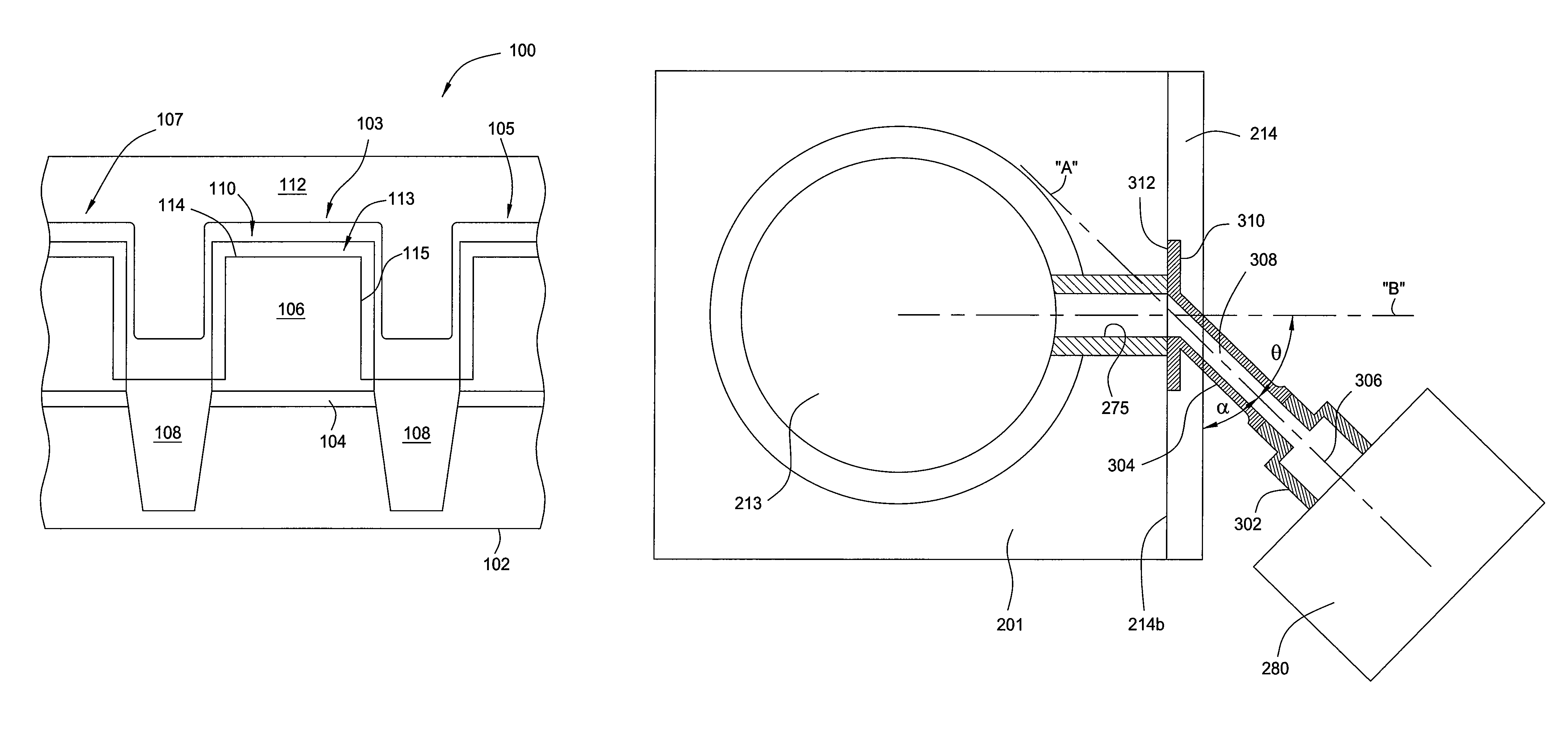
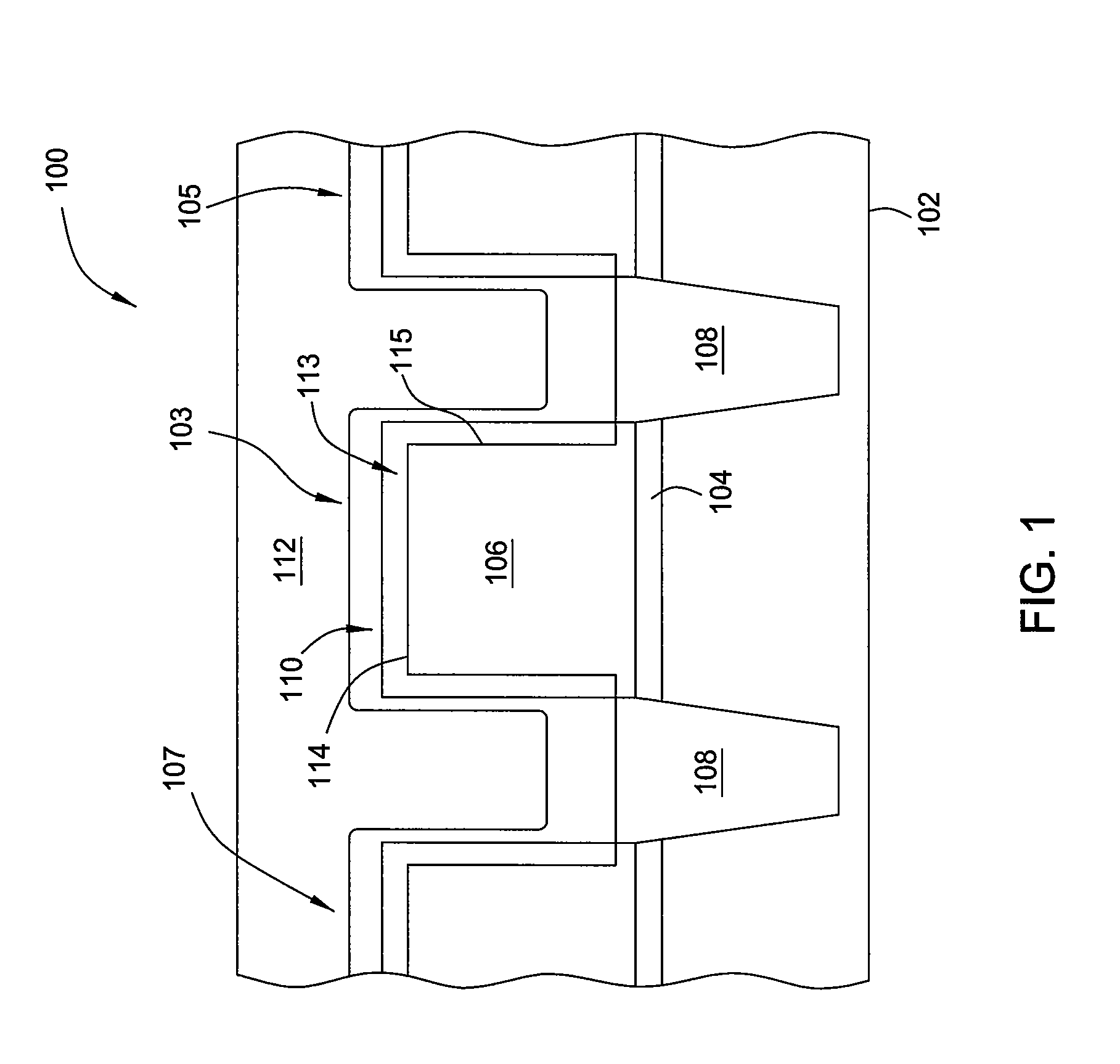
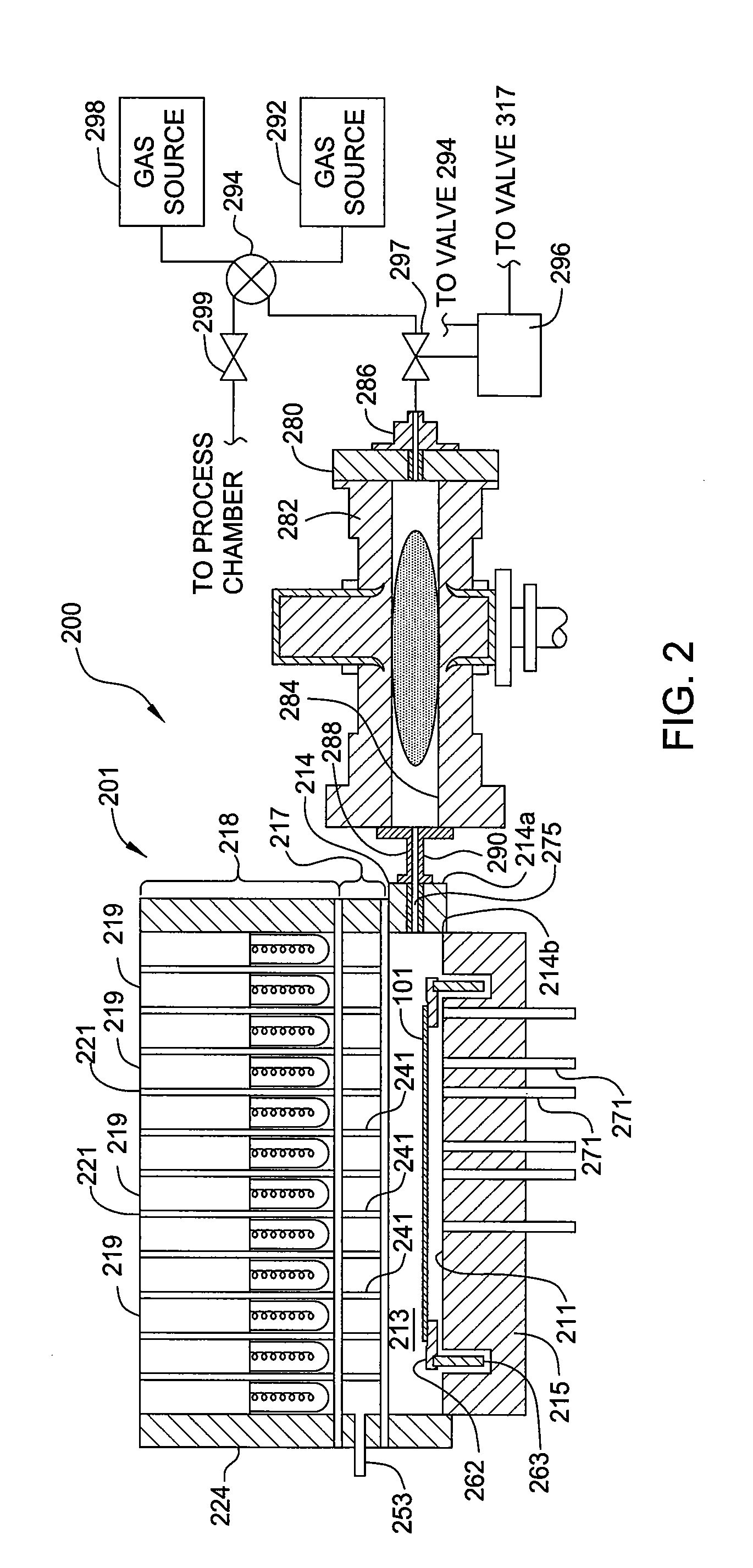
[0018]The invention describes an apparatus and method for incorporating radicals of a plasma into a substrate or a material on a semiconductor substrate using a remote plasma source. In general, plasma sources generated by, for example, an energetic excitation of gaseous molecules consisting of a plasma of charged ions, radicals, and electrons. The inventors of the present invention recognize that radicals of a plasma react in a much more desirable manner with silicon or polysilicon material on a substrate, than ions or a mixture of radicals and ions. In that regard, the invention provides an apparatus and a method of eliminating the majority of the ions of the plasma such that only radicals of the plasma react with silicon or polysilicon material on a substrate, thereby obtaining a greater selectivity of processing of silicon or polysilicon material on the substrate.

[0019]The present invention is not intended to be limited to a particular device since the apparatus and methods desc...


PUM


Abstract

Embodiments described herein generally relate to methods for manufacturing flash memory devices. In one embodiment, the method includes generating a plasma comprising nitrogen-containing radicals in a remote plasma applicator, flowing the plasma comprising nitrogen-containing radicals into a processing region of the processing chamber where a semiconductor device is disposed, wherein the semiconductor device has a substrate comprising an oxide layer formed thereon, exposing an exposed surface of the oxide layer to the nitrogen-containing radicals, and incorporating nitrogen in the exposed surface of the oxide layer of the substrate.

Description

CROSS-REFERENCE TO RELATED APPLICATIONS[0001]This application claims benefit of U.S. provisional patent application Ser. No. 61 / 552,370, filed Oct. 27, 2011, which is herein incorporated by reference.BACKGROUND[0002]1. Field of the Invention[0003]Embodiments of the present invention generally relate to manufacturing semiconductor devices. More specifically, embodiments described herein relate to manufacture of floating gate NAND memory devices and other transistor gate dielectrics using an improved plasma applicator and process.[0004]2. Description of the Related Art[0005]Flash memory, such as NAND flash memory devices, is a commonly used type of non-volatile memory in widespread use for mass storage applications. The NAND flash memory devices typically have a stacked type gate structure in which a tunnel oxide (TO), a floating gate (FG), an inter-poly dielectric (IPD), and a control gate (CG) are sequentially stacked on a semiconductor substrate. The floating gate, the tunnel oxide...

Claims


Application Information

Patent Timeline
Patent Type & Authority Patents(United States)
IPC IPC(8): H01L21/31
CPCH01L21/0217H01L27/11524H01L21/02247H01L21/02252H01L21/0234H01L21/28273H01L21/02332H01L21/02164H01L21/3211H01J37/32357H01L21/3115H01J37/32422H01L29/40114H10B41/35
Inventor OLSEN, CHRISTOPHER S.YOKOTA, YOSHITAKA
Owner APPLIED MATERIALS INC
Why Eureka
Try Eureka