

Three-dimensional non-volatile memory device
a memory device, non-volatile technology, applied in the direction of semiconductor devices, digital storage, instruments, etc., can solve the problems of complex operation methods, physical limits in increasing the degree of integration of memory cells, and two-dimensional memory devices in which memory cells are manufactured, and achieve the effect of simple methods
- Summary
- Abstract
- Description
- Claims
- Application Information
AI Technical Summary
Benefits of technology
Problems solved by technology
Method used
Image

Examples
first embodiment
[0056]FIGS. 3A and 3B are views illustrating the structure of a semiconductor device according to the present invention. FIG. 3A is a layout view of a cell array. FIG. 3B is a circuit diagram of a portion of the cell array of FIG. 3A.
[0057]As shown in FIG. 3A, one of the memory blocks MB of the semiconductor device according to the first embodiment of the present invention may include M string rows ST_ROW1 to ST_ROWM that extend in the first direction I-I′. In addition, each of the string rows ST_ROW1 to ST_ROWM may include 2N strings ST1 to ST2N.
[0058]In particular, according to the first embodiment, first to 2N-th strings ST1 to ST2N, included in the string row ST_ROW1, may be alternately coupled to odd and even bit lines O_BL1 and E_BL1. Therefore, when first to 2N-th channel layers of the first to 2N-th strings ST1 to ST2N are arranged in a sequential manner, the first channel layer may be aligned with the third channel layer while the second channel layer may be aligned with th...
second embodiment
[0075]As shown in FIG. 4A, one of the memory blocks MB of the semiconductor device according to the present invention may include six string rows ST_ROW1 to ST_ROW6. Each of the string rows ST_ROW1 to ST_ROW6 may include four strings ST1 to ST4.
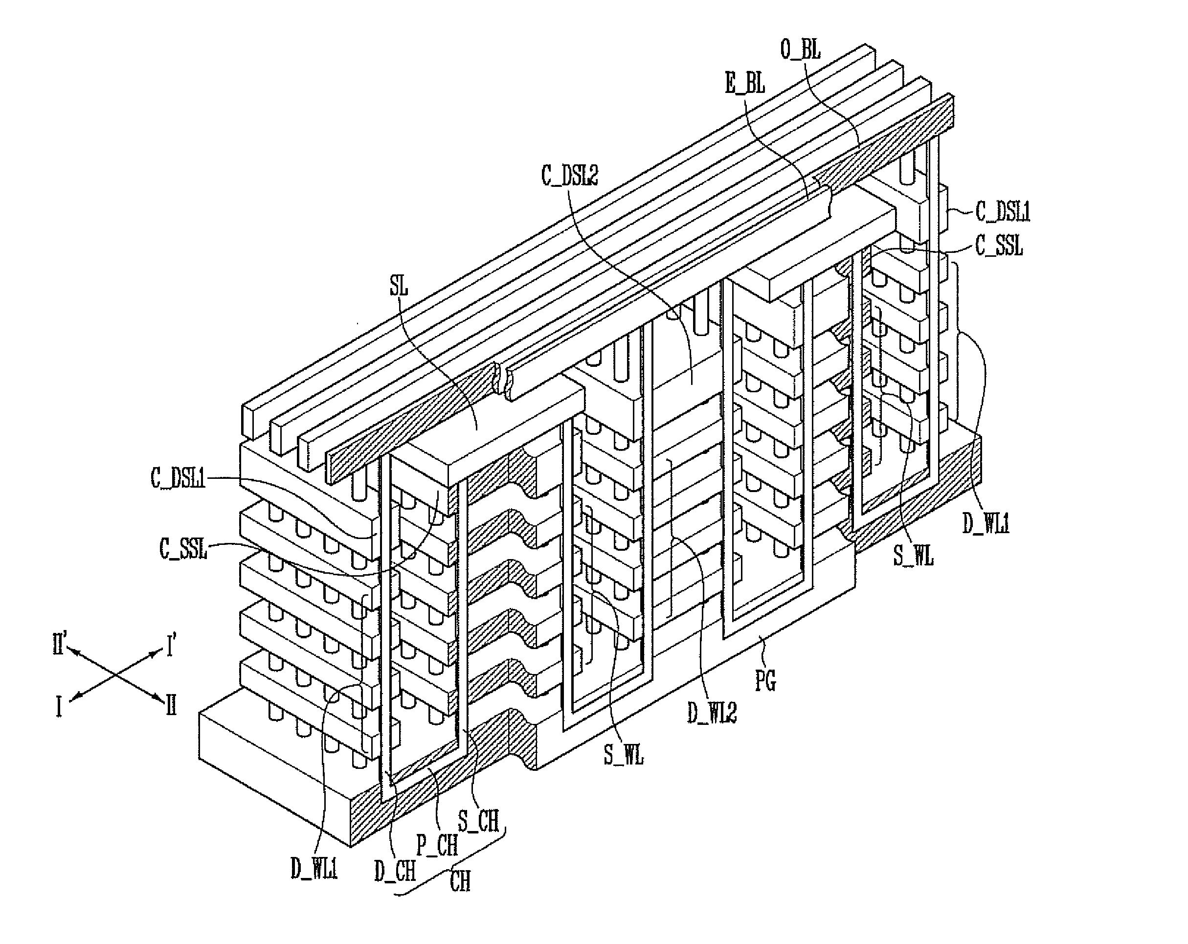
[0076]As shown in FIG. 4B, source selection transistors SST of the strings ST1 to ST4, included in the memory block MB, may be controlled by one common source selection line C_SSL.
[0077]In addition, the drain selection transistors DST of the first string ST1 and the fourth string ST4, among the strings ST1 to ST4 included in the memory block MB, may be controlled by one first common drain selection line C_DSL1. In addition, the drain selection transistors DST of the second string ST2 and the third string ST3 may be commonly controlled by one second common drain selection line C_DSL2.
[0078]Therefore, during a program operation or a read operation, the memory cells MC of the first string ST1 and the fourth string ST4 that are disposed at the sa...
third embodiment
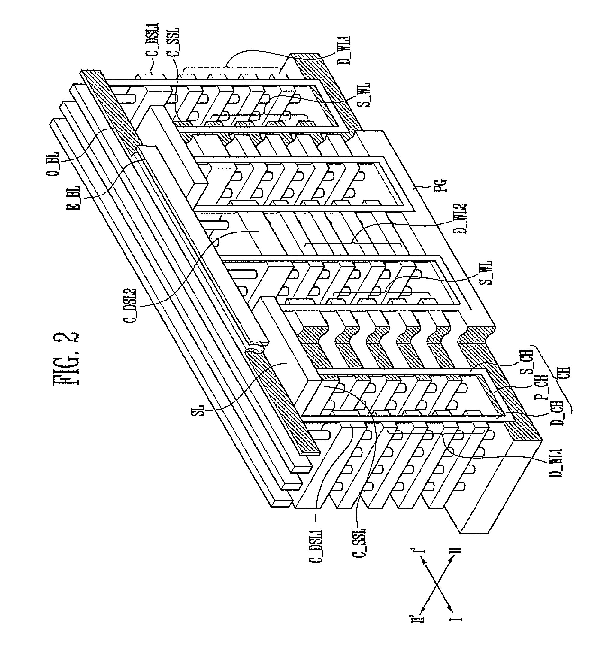
[0081]As shown in FIG. 5A, one memory block MB of the semiconductor device according to the present invention may include six string rows ST_ROW1 to ST_ROW6. Each of the string rows, for example, the string row ST_ROW1 may include six strings ST1 to ST6.
[0082]Here, common source selection line layers C_SSL1 to C_SSL3 that are disposed at the same level may have separate patterns and be separately operated. In particular, source selection transistors of adjacent strings ST1 / ST2, ST3 / ST4 and ST5 / ST6, among the strings ST1 to ST6 included in the string row ST_ROW1, may be commonly controlled by the common source selection lines C_SSL1, C_SSL2 and C_SSL3, respectively.
[0083]As shown in FIG. 5B, the source selection transistors SST of the strings ST1 to ST6 included in the memory block MB may be controlled by the common source selection lines C_SSL1, C_SSL2 and C_SSL3. Therefore, the source selection transistors SST of the first and second strings ST1 and ST2 may be controlled by the com...
PUM
 Abstract
Description
Claims
Application Information