Semiconductor device

a technology of semiconductor devices and mosfets, which is applied in the direction of semiconductor devices, semiconductor/solid-state device details, electrical apparatus, etc., can solve the problems of short circuit between gate g and source s, short circuit between a trap member and a gate g, and the inability to use the power mosfet for synchronous rectification

Inactive Publication Date: 2004-02-12
KK TOSHIBA
View PDF3 Cites 18 Cited by
  • Summary
  • Abstract
  • Description
  • Claims
  • Application Information

AI Technical Summary

Problems solved by technology

Unfortunately, in reliability tests such as a temperature cycle test for a power MOSFET, this strap member structure shortens the life of the power MOSFET because the thermal expansion coefficients of an Al electrode on the chip surface, the Ag paste, the Cu s

Method used


Image

  • Semiconductor device
  • Semiconductor device
  • Semiconductor device

Examples


first embodiment

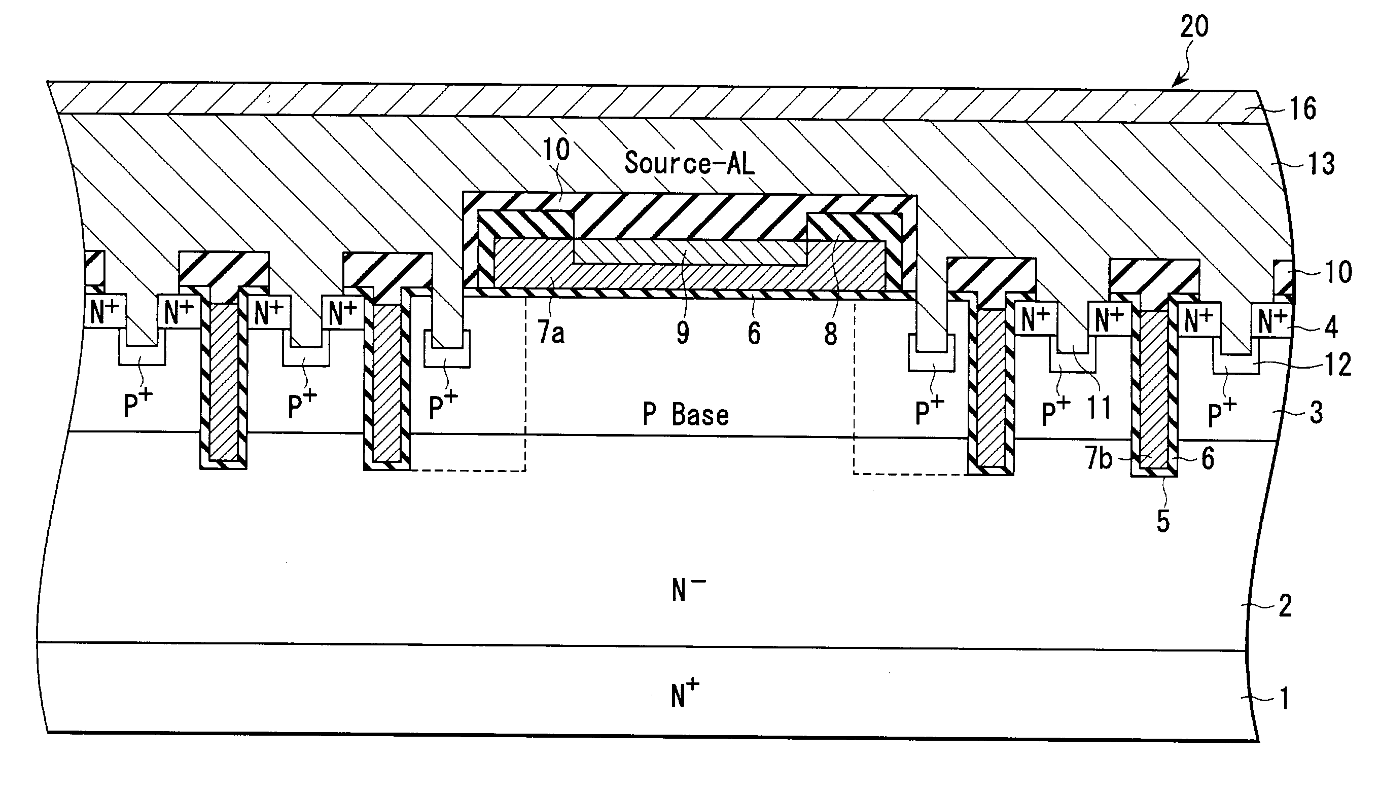
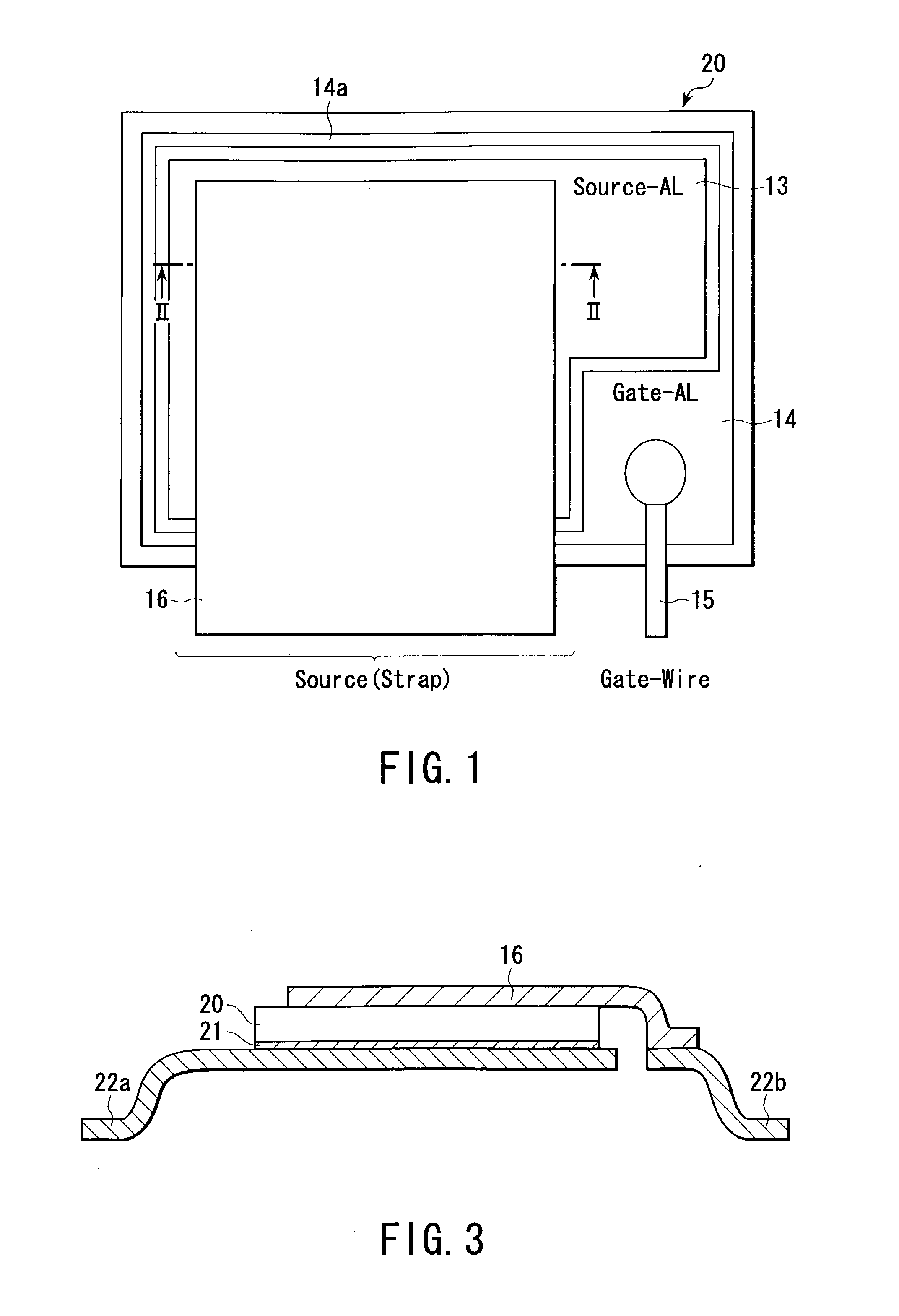
[0028] FIG. 1 is a plan view schematically showing a portion of a trench gate type power N(-channel) MOSFET using a strap member according to the FIG. 2 is a sectional view schematically showing a structure taken along a line II-II in FIG. 1.

[0029] In this power MOSFET shown in FIGS. 1 and 2, a semiconductor chip 20, which includes a MOSFET having a surface source electrode 13 connected to source diffusion layers 4 and a surface gate electrode 14 connected to a gate polysilicon wiring layer 7a, is mounted on a lead frame as shown in FIG. 3.

[0030] A wire (Gate-Wire) 15 is connected by bonding so as to electrically connect the surface gate electrode 14 to a lead portion of the lead frame.

[0031] In addition, to electrically connect the surface source electrode 13 to the lead frame, a Cu or Al strap member 16 is connected onto the surface source electrode 13 by US.

[0032] In the semiconductor chip 20, reference numeral 1 denotes an N.sup.+-type silicon substrate; 2, an N-type epitaxial ...

second embodiment

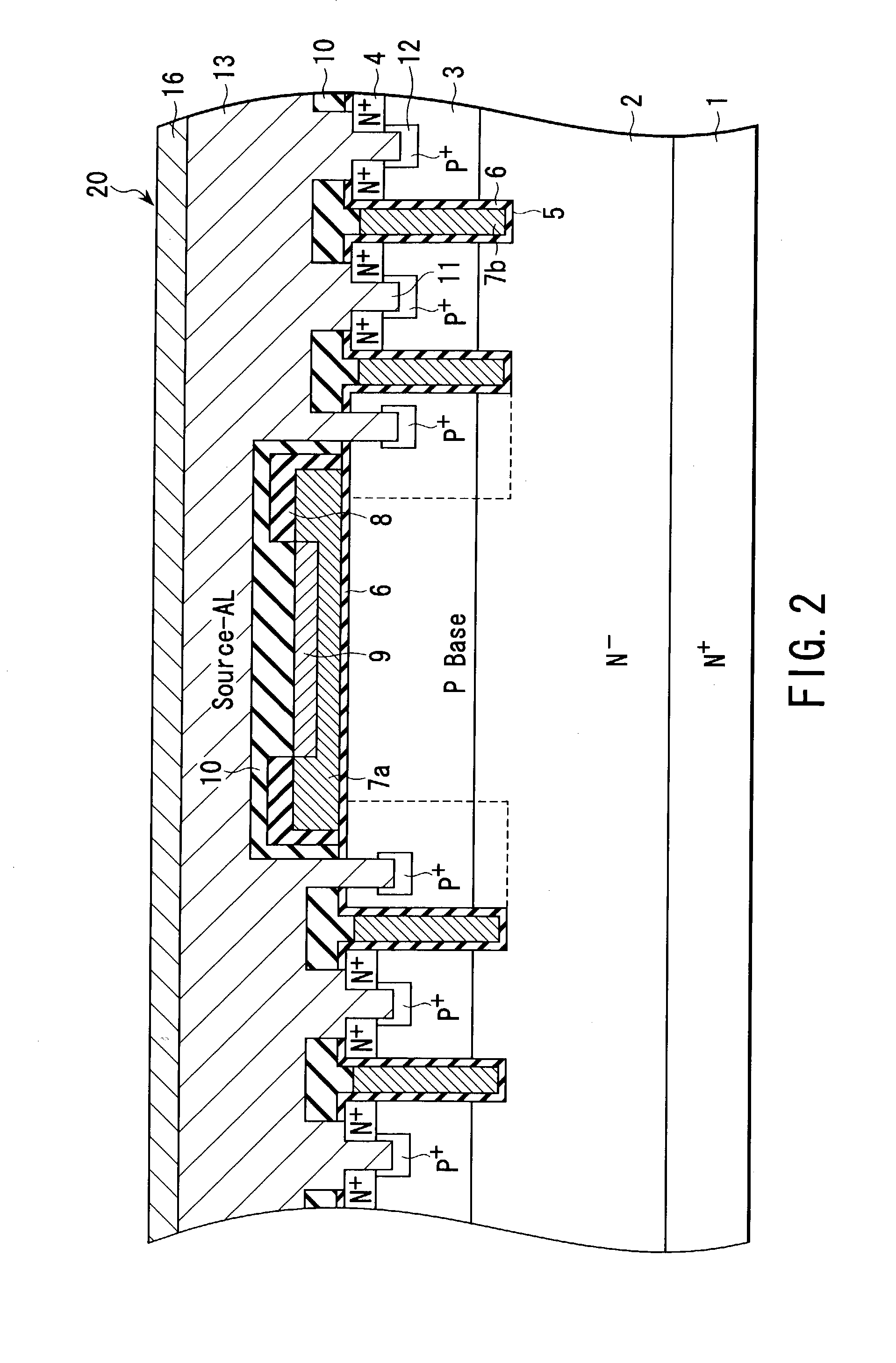
[0050] FIG. 4 is a sectional view schematically showing a portion of a trench gate type NMOSFET using a strap member according to the

[0051] This power NMOSFET of the second embodiment has the same planar pattern as the power NMOSFET of the first embodiment described above. However, the sectional structure and formation steps of a gate polysilicon wiring layer are different as will be described below. Since the rest is the same, the same reference numerals as in FIG. 2 denote the same parts in FIG. 4.

[0052] That is, the polysilicon film for the gate electrode, which is heavily doped with the N-type impurity, is deposited until gate trenches 5 are completely filled, and this polysilicon film is selectively etched to the silicon surface except for the gate wiring layer portion, thereby forming the gate polysilicon wiring layer 7a and trench gates 7b. These processes are the same as in the first embodiment. Thereafter, Ti / TiN, for example, is deposited by sputtering without depositing a...


PUM


Abstract

A semiconductor device comprising a semiconductor substrate having first and second surfaces opposing each other, the substrate including a plurality of cells sharing a common drain region, each of the cells having source and gate regions, a surface source electrode connected to the source region of each of the cells and provided on the first surface, a strap member coupled with the surface source electrode by ultrasonic waves, a gate polysilicon wiring layer connecting the gate region of each of the cells and having a silicide layer in at least a portion of a surface thereof, a surface gate electrode connected to the gate polysilicon wiring layer and provided on the first surface, and a drain electrode provided on the second surface and shared by the cells.

Description

[0001] This application is based upon and claims the benefit of priority from the prior Japanese Patent Application No. 2002-141495, filed May 16, 2002, the entire contents of which are incorporated herein by reference.[0002] 1. Field of the Invention[0003] The present invention relates to a semiconductor device and, more particularly, to a semiconductor device in which a surface source electrode of a MOSFET (insulated gate field-effect transistor) is electrically connected to a lead frame via a strap member. For example, the present invention is used in a trench gate type power MOSFET.[0004] 2. Description of the Related Art[0005] FIG. 5 is a plan view schematically showing a portion of a conventional trench gate type power MOSFET using a wire bonding structure. FIG. 6 is a sectional view schematically showing a structure taken along a line VI-VI in FIG. 5.[0006] This power MOSFET is comprised of a plurality of MOSFET cells, and includes a surface source electrode (Source-AL) 13 co...

Claims


Application Information

Patent Timeline
IPC IPC(8): H01L23/482H01L23/495H01L29/41H01L29/417H01L29/423H01L21/28H01L29/49H01L29/739H01L29/78
CPCH01L23/4824H01L24/49H01L29/41741H01L29/41766H01L29/4941H01L29/7802H01L29/7813H01L23/49562H01L2224/32245H01L2224/73221H01L2224/40247H01L2224/04042H01L24/05H01L24/06H01L24/34H01L2224/05624H01L2224/0603H01L2224/48247H01L2224/48465H01L2224/4911H01L2224/73265H01L2924/15747H01L2224/37124H01L2224/37147H01L2924/13055H01L2924/13091H01L2924/1305H01L2924/1306H01L2224/48463H01L2224/05552H01L2924/00H01L2924/00014H01L24/40H01L2224/40245H01L24/37H01L2224/40091H01L24/48H01L2224/84205H01L24/84H01L2224/45099H01L2224/05599
Inventor MATSUKI, HIROBUMITAKANO, AKIOKAWANO, TAKAHIRO
Owner KK TOSHIBA
Why Eureka
Try Eureka