Multi-transistor layout capable of saving area

a multi-transistor, saving area technology, applied in the direction of semiconductor devices, semiconductor/solid-state device details, electrical apparatus, etc., can solve the problems of increasing the reaction time of current-steering dac and reducing efficiency, and achieve the effect of saving area

Active Publication Date: 2007-11-13
FARADAY TECH CORP
View PDF3 Cites 18 Cited by
  • Summary
  • Abstract
  • Description
  • Claims
  • Application Information

AI Technical Summary

Benefits of technology

[0009]It is therefore a primary objective of the claimed invention to provide multi-transistor layouts capable of saving area.
[0012]The present invention further discloses a multi-transistor layout capable of saving area, which includes: a substrate; a common drain array on the substrate comprising a plurality of common drains, each comprising four sides; a plurality of gates formed over four sides of each common drain of the plurality of the common drains; and a plurality of common sources formed between adjacent gates of the plurality of the gates.

Problems solved by technology

Therefore, in an output end of a current-steering DAC, a drain of a transistor switch occupies a large area, induces parasitic capacitance, increases reaction time of the current-steering DAC, and decreases efficiency.

Method used


Image

  • Multi-transistor layout capable of saving area
  • Multi-transistor layout capable of saving area
  • Multi-transistor layout capable of saving area

Examples


Embodiment Construction

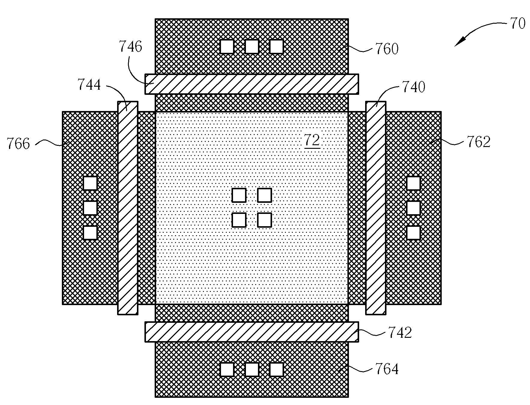
[0025]Please refer to FIG. 7, which illustrates a schematic diagram of a multi-transistor layout 70 in accordance with the present invention. The multi-transistor layout 70 includes a common drain 72, gates 740, 742, 744, 746, and sources 760, 762, 764, 766. The common drain 72 includes four contacts, each of the gates 740, 742, 744, and 746 includes one contact, and each of the sources 760, 762, 764, and 766 includes three contacts. If a minimum acceptable width of a drain is 4 μm and areas of the contacts on the common drain 72 are considered, a drain of a transistor in the multi-transistor layout 70 occupies an area of 7.02 μm2 (=5.3 μm×5.3 μm×0.25, where “0.25” means that four transistors share one drain). Therefore, the area of each drain in the present invention multi-transistor layout 70 is 31% of that in the multi-transistor layout 30. That is, for the same ESD rule, in a fixed area, the present invention multi-transistor layout 70 can save area and can be applied for a circ...


PUM


Abstract

A multi-transistor layout capable of saving area includes a substrate; a common drain comprising four sides formed over the substrate; four gates formed over the four sides of the common drain; and four sources formed over outer sides of the four gates corresponding to the common drain.

Description

BACKGROUND OF INVENTION[0001]1. Field of the Invention[0002]The present invention provides a multi-transistor layout capable of saving area, and more particularly, a multi-transistor layout with common drains.[0003]2. Description of the Prior Art[0004]As manufacturing processes of VLSI (very large scale integrated) circuits improves, operating frequencies of microprocessors, wireless communication units, etc. become higher and higher. In order to meet such high-frequency demand, improved efficiency of digital to analog converts, or DACs, is expected. In the prior art, a current-steering DAC is a high-speed DAC, whose signal current is switched to different outputs through switch gates.[0005]Please refer to FIG. 1, which illustrates a schematic diagram of a prior art current-steering DAC 10. The current-steering DAC 10 includes common-source differential pairs S1, S2 to SN and corresponding current sources I1, I2 to IN. Each of the common-source differential pairs S1, S2 to SN includ...

Claims


Application Information

Patent Timeline
Patent Type & Authority Patents(United States)
IPC IPC(8): H01L23/62H01L29/76H01L29/94H01L31/062H01L31/113
CPCH01L29/78H01L29/41725H01L29/0692H01L27/0266
Inventor CHEN, HSIN-HUNG
Owner FARADAY TECH CORP
Why Eureka
Try Eureka