Static random access memory

a random access and memory technology, applied in the field of static random access memory, can solve the problem of frequent occurrence of software errors in the conventional sram cell, and achieve the effect of improving the software error resistance of such a sram cell

Inactive Publication Date: 2006-06-06
KK TOSHIBA
View PDF3 Cites 19 Cited by
  • Summary
  • Abstract
  • Description
  • Claims
  • Application Information

AI Technical Summary

Benefits of technology

[0009]An object of the present invention is to improve software error resistance of such an SRAM cell.

Problems solved by technology

The conventional SRAM has a problem of frequent occurrence of a software error due to a rays or neutrons having entered the depletion layer within the substrate of the field-effect transistor.

Method used


Image

  • Static random access memory
  • Static random access memory
  • Static random access memory

Examples


first embodiment

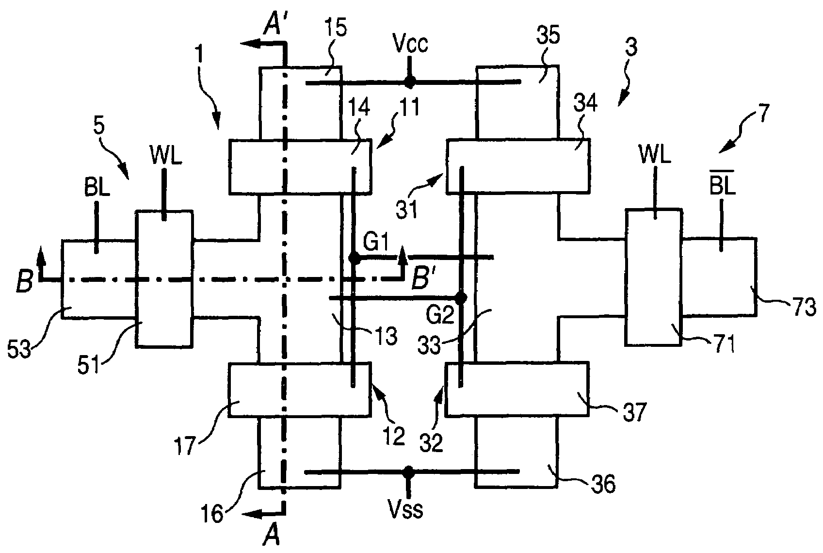
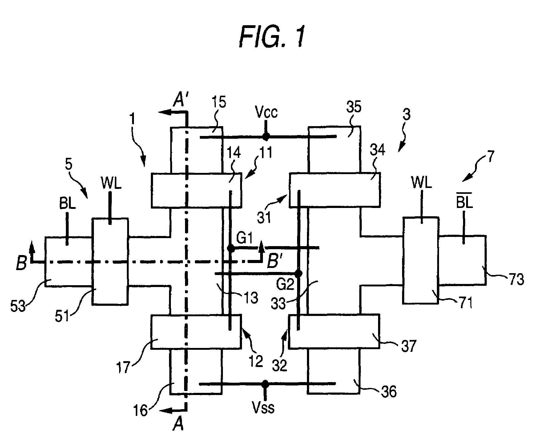
[0023]FIG. 1 shows a top view of an SRAM memory cell according to an embodiment of the present invention.

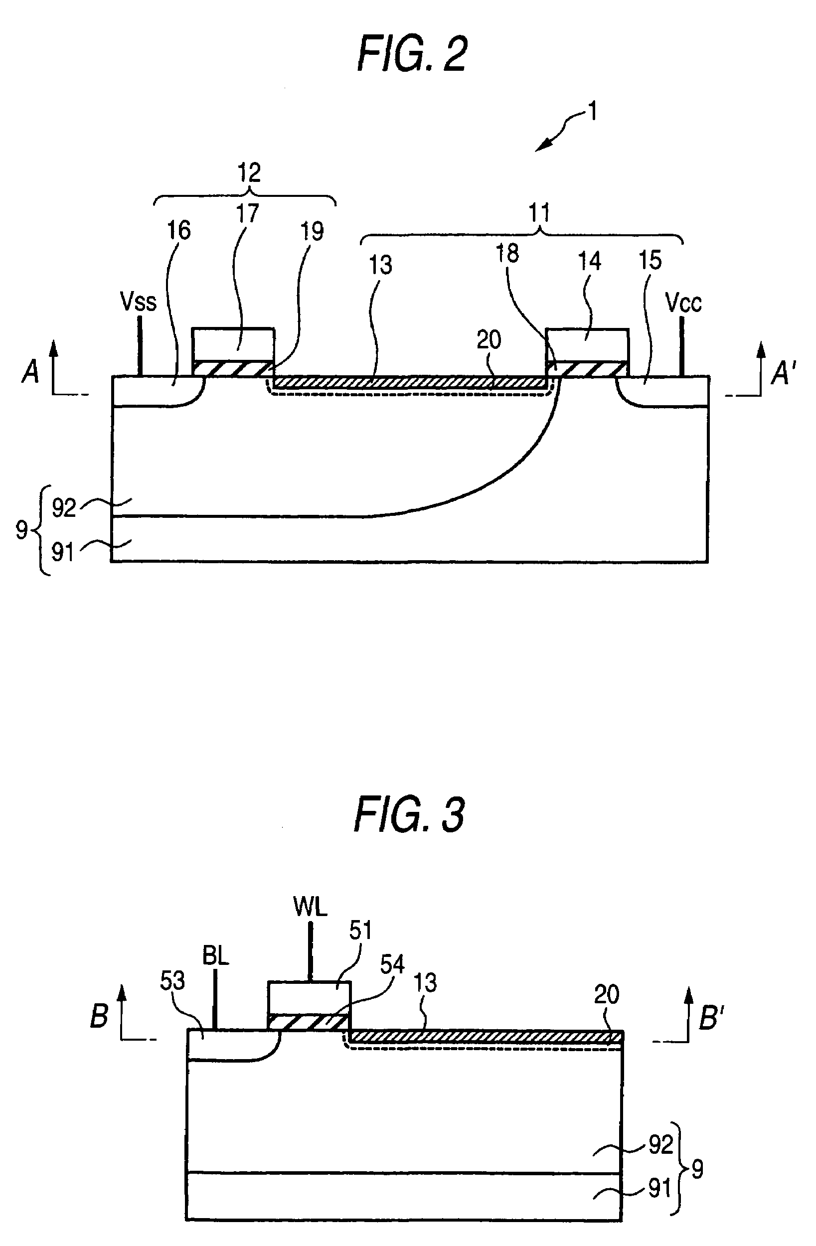
[0024]This SRAM memory cell has a first CMOS 1 and a second CMOS 3. The first CMOS 1 has a field-effect transistor 11 of positive hole conduction type and a field-effect transistor 12 of electron conduction type, which share a drain region 13. A gate electrode 14 of the field-effect transistor 11 of positive hole conduction type and a gate electrode 17 of the field-effect transistor 12 of electron conduction type are connected together (made common to the gate electrodes 14, 17) by means of an interconnection G1. Reference numeral 15 designates a source region of the field-effect transistor 11 of positive hole conduction type; and 16 designates a source region of the field-effect transistor 12 of electron conduction type.

[0025]The second CMOS 3 has a field-effect transistor 31 of positive conduction type and a field-effect transistor 32 of electron conduction type, which share a ...

second embodiment

[0043]A Schottky drain SRAM according to a second embodiment of the present invention will be described by reference to a top view shown in FIG. 7.

[0044]In this embodiment, the gate electrode 14 of the field-effect transistor of positive hole conduction type and the gate electrode 17 of field-effect transistor of electron conduction type, both belonging to the first CMOS 1, are connected together by means of an upper conductor layer M0, thereby forming a common gate of the first CMOS 1. This upper conductor layer M0 is connected to the drain region 33 of the second CMOS 3 by means of an upper conductor M1′.

[0045]The gate electrode 34 of positive hole conduction type of the second CMOS 3 is connected to the gate electrode 37 of electron conduction type by means of the upper conduction layer M0′ and further to the drain region 13 of the first CMOS 1 by means of an upper conductor M1.

[0046]When the drain region of the CMOS and the drain region pertaining to the field-effect transistor ...


PUM


Abstract

A static random access memory has first and second complementary field-effect transistors. The first complementary field-effect transistor includes a semiconductor substrate, a first field-effect transistor of electron conduction type which has a first drain region constituting a Schottky junction and a gate electrode, and a first field-effect transistor of positive hole conduction type which shares the first drain region and has a shared gate electrode. The second complementary field-effect transistor includes a second field-effect transistor of electron conduction type which has a second drain region and a gate electrode, a second field-effect transistor of positive hole conduction type which shares the second drain region and has a shared gate electrode. The gate electrode shared by the first and second complementary field-effect transistors is connected to the common drain region of the mutually opposing complementary field-effect transistors, and the static random access memory has superior resistance to software errors.

Description

CROSS-REFERENCE TO RELATED APPLICATIONS[0001]This application is based upon and claims the benefit of priority from the prior Japanese Patent Application No. 2003-332107, filed Sep. 24, 2003, the entire contents of which are incorporated herein by reference.BACKGROUND OF THE INVENTION[0002]1. Field of the Invention[0003]The present invention relates to static random access memory (hereinafter called “SRAM”) equipped with a complementary field-effect transistor.[0004]2. Background Art[0005]One of high-speed, power-thrifty semiconductor memory devices is SRAM formed from a complementary metal-oxide-semiconductor field-effect transistor (hereinafter abbreviated as CMOS). The CMOS has a field-effect transistor of electronic conduction type and a field-effect transistor of hole conduction type. Each memory cell of the SRAM has two CMOS devices, and a field-effect transistor constituting a transfer gate connected to the respective CMOS devices.[0006]In such a field-effect transistor, when...

Claims


Application Information

Patent Timeline
Patent Type & Authority Patents(United States)
IPC IPC(8): H01L27/11H01L29/417H01L21/8244H01L27/08H01L27/092H01L27/146H01L27/148
CPCH01L27/11H01L27/1104Y10S257/903H01L27/1463H10B10/00H10B10/12
Inventor MATSUZAWA, KAZUYAUCHIDA, KENNAKAUCHI, TAKAHIRO
Owner KK TOSHIBA
Why Eureka
Try Eureka