Duty cycle correction circuit

a duty cycle and circuit technology, applied in the direction of generating/distributing signals, pulse manipulation, pulse techniques, etc., can solve the problems of error db>3/b> cannot be neglected, and become difficult to provide a clock signal with a 50% duty cycl

Inactive Publication Date: 2006-01-03
PANASONIC CORP
View PDF7 Cites 18 Cited by
  • Summary
  • Abstract
  • Description
  • Claims
  • Application Information

AI Technical Summary

Benefits of technology

[0018]Thus, either the n-channel or p-channel transistor is provided in the delay circuit and the first clock signal is passed between the source and drain of the transistor. This enables delay of the first clock signal.

Problems solved by technology

With such trend, it becomes difficult to provide a clock signal with a 50% duty cycle because of the effect of signal propagation delay caused by transistors constituting the frequency divider circuit 100, especially the effect of delay caused by the MOS resistances.
However, as the frequencies thereof become higher, the error d3 cannot be neglected.

Method used


Image

  • Duty cycle correction circuit
  • Duty cycle correction circuit
  • Duty cycle correction circuit

Examples


first embodiment

(First Embodiment)

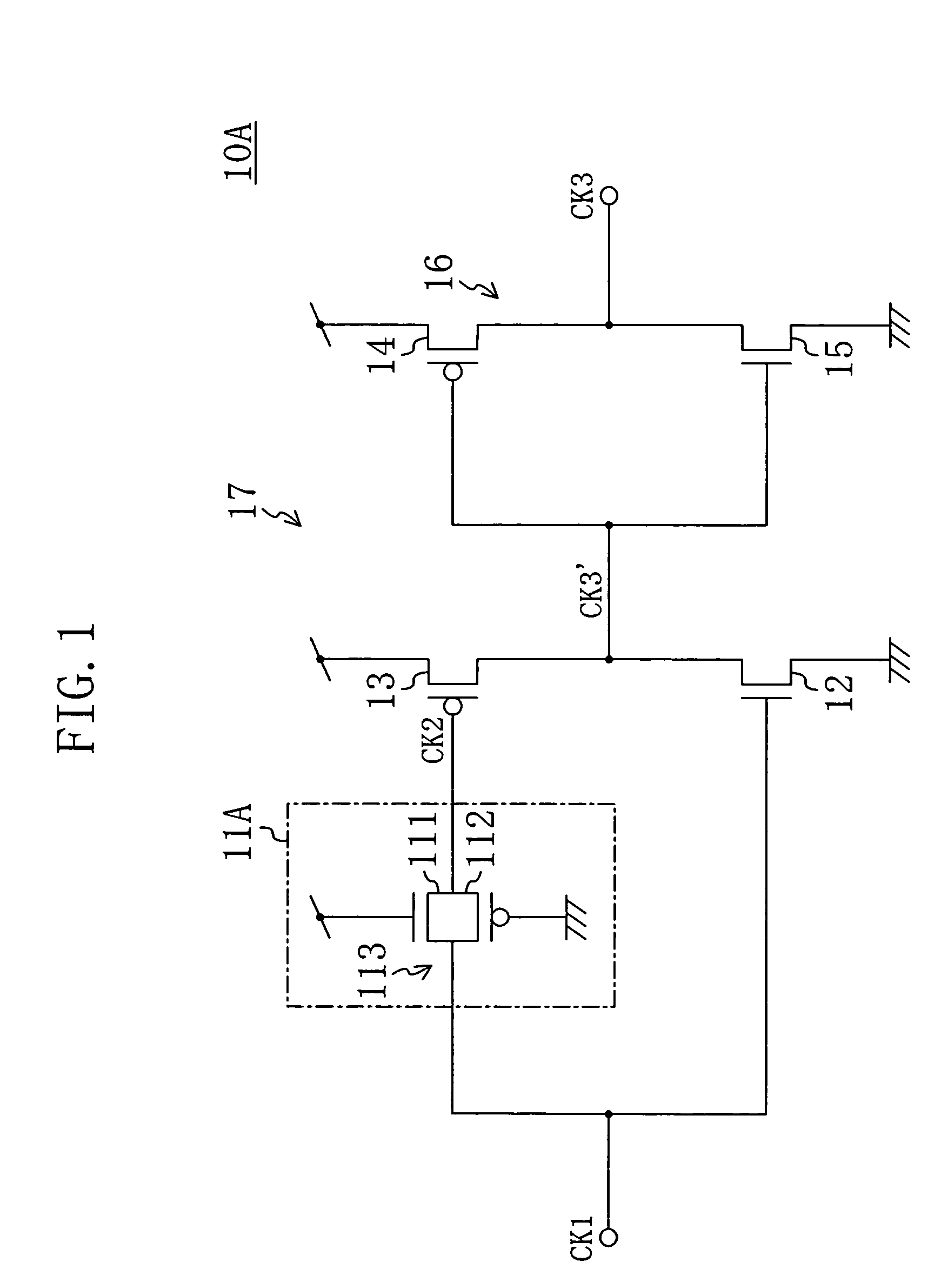
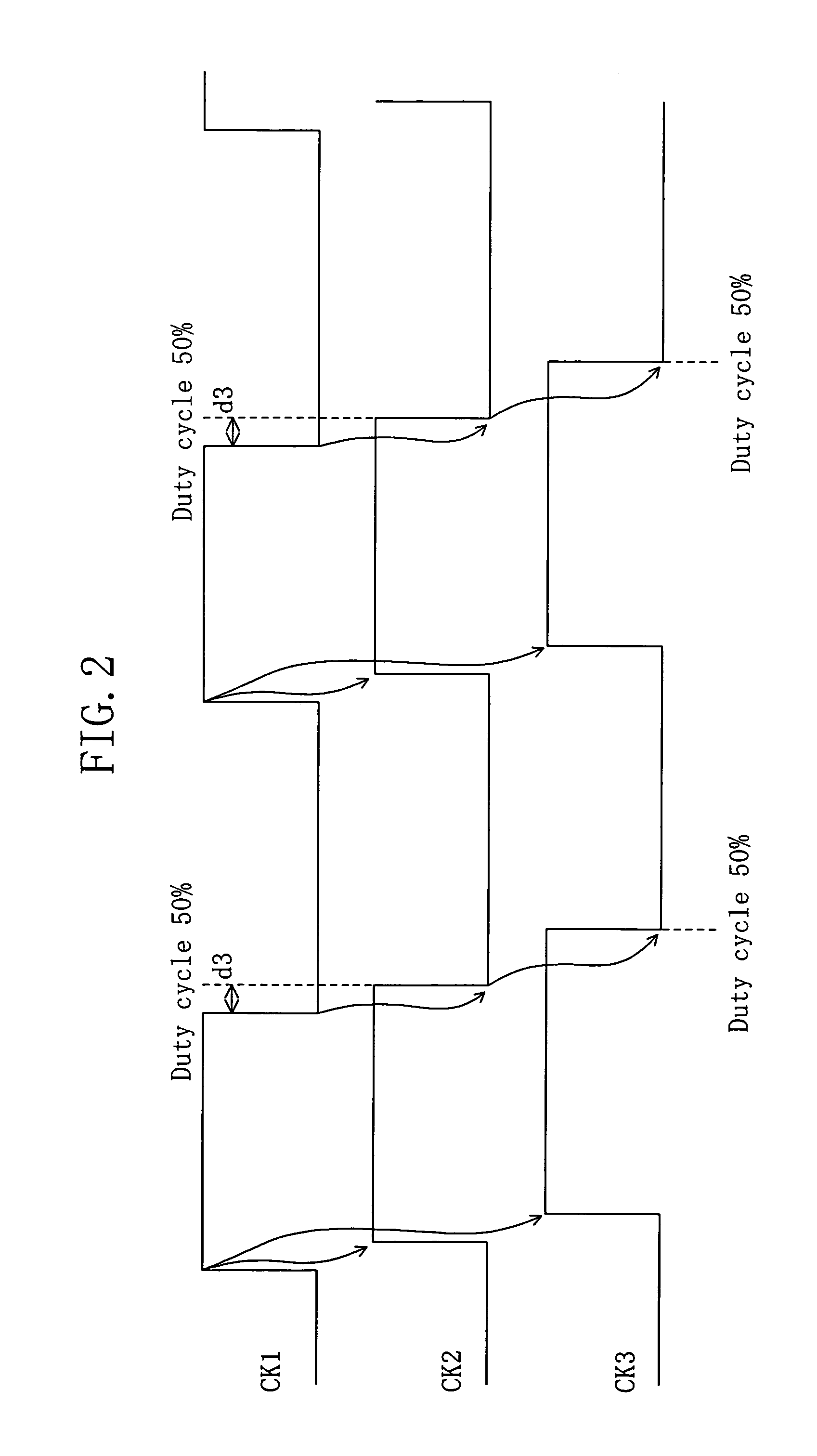
[0031]FIG. 1 shows a circuit configuration of a duty cycle correction circuit according to a first embodiment of the present invention. A duty cycle correction circuit 10A of this embodiment includes a delay unit 11A, an n-channel transistor 12, a p-channel transistor 13, and an inverter circuit 16. The delay unit 11A delays a clock signal CK1 (corresponding to a first clock signal) which is given to the duty cycle correction circuit 10A to output a clock signal CK2 corresponding to a second clock signal. The n-channel transistor 12 has a source supplied with a ground voltage and a gate supplied with the clock signal CK1. The p-channel transistor 13 has a source supplied with a source voltage and a gate supplied with the clock signal CK2. The inverter circuit 16 is composed of transistors 14 and 15 and inverses a signal CK3′ output by a common drain of the transistors 12 and 13 to output a clock signal CK3 corresponding to a third clock signal. In addition, the tra...

second embodiment

(Second Embodiment)

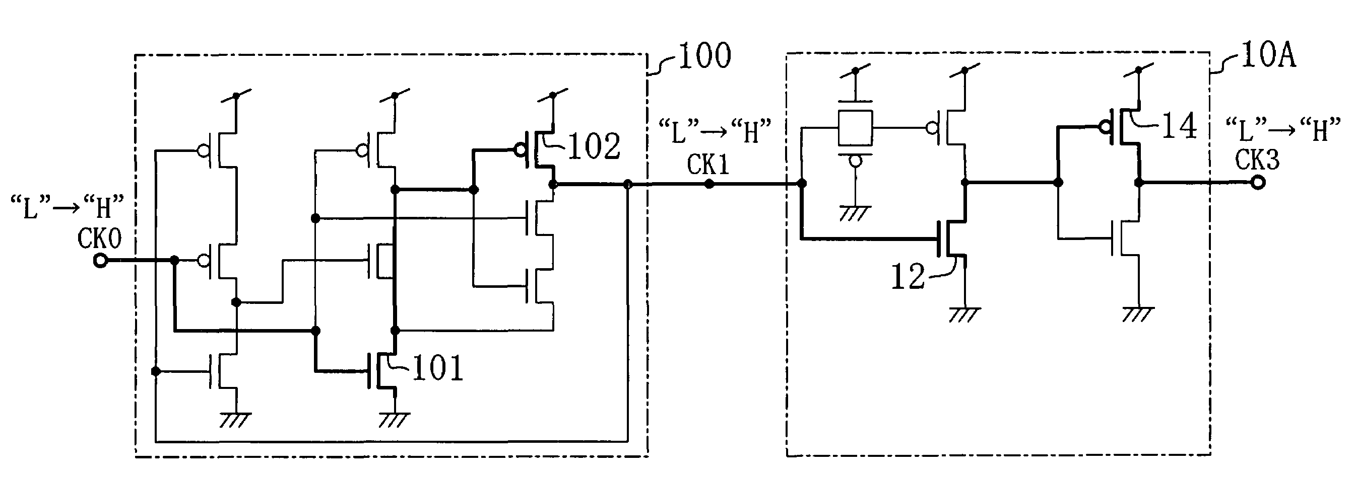
[0047]FIG. 4 shows a circuit configuration of a duty cycle correction circuit according to a second embodiment of the present invention. A duty cycle correction circuit 10B of this embodiment is configured by replacing the delay unit 11A of the duty cycle correction circuit 10A according to the first embodiment with a delay unit 11B having a different circuit configuration from the delay unit 11A. The duty cycle correction circuit 10B also includes a clock-signal output unit 18 with the same circuit configuration as the duty cycle correction circuit 10A but the absence of the inverter circuit 16. The clock-signal output unit 18 outputs the signal CK3′ shown in FIG. 1 as the clock CK3. The description of the components shown in FIG. 4 that are the same as those shown in FIG. 1 will be omitted by retaining the same reference numerals. Hereinafter, only the delay unit 11B will be described.

[0048]The delay unit 11B has a transfer gate 113 composed of an n-channel tran...

third embodiment

(Third Embodiment)

[0052]FIG. 5 shows a circuit configuration of a duty cycle correction circuit according to a third embodiment of the present invention. A duty cycle correction circuit 10C of this embodiment is configured by replacing the delay unit 11B of the duty cycle correction circuit 10B according to the second embodiment with a delay unit 11C having a different circuit configuration from the delay unit 11B. The description of the components shown in FIG. 5 that are the same as those shown in FIG. 4 will be omitted by retaining the same reference numerals. Hereinafter, only the delay unit 11C will be described.

[0053]The delay unit 11C has a p-channel transistor 112. A gate of the transistor 112 is supplied with a gate threshold voltage Vth of the transistor 112. Since the transistor 112 is of p-channel type, the voltage supplied thereto is lower than the ground voltage. Thus, by supplying the gate of the transistor 112 with the gate threshold voltage Vth, the switching operat...


PUM


Abstract

In order to correct the duty cycle of a given clock signal to produce a clock signal with a 50% duty cycle, a duty cycle correction circuit includes a delay unit for delaying a first clock signal to output a second clock signal and a clock-signal output unit. The clock-signal output unit includes two transistors which use the first and second clock signals as the inputs of respective gates and an inverter circuit for inverting a signal output from a common drain of the transistors to output a third clock signal. The delay unit delays the first clock signal so that the first clock signal falling appears at a timing at which the duty cycle thereof becomes 50%. The two transistors in the clock-signal output unit output, as the third clock signal, a ground voltage and a source voltage as the signal from the common drain in response to the rising of the first clock signal and the falling of the second clock signal, respectively.

Description

BACKGROUND OF THE INVENTION[0001]1. Field of the Invention[0002]The present invention relates to circuits for processing a clock signal in a digital circuit. Specifically, the present invention relates to circuit techniques suitable for correction of the duty cycle of a clock signal produced by a frequency divider circuit or the like.[0003]2. Description of the Related Art[0004]For digital circuits, it is of great importance to keep a clock signal, which is used for synchronizing the operations of various units in the circuit, in a 50% duty cycle. Generally, a clock signal with a 50% duty cycle is produced by a frequency divider circuit.[0005]FIG. 7 shows a typical circuit configuration of the frequency divider circuit (a divide-by-two frequency divider circuit). A frequency divider circuit 100 shown in FIG. 7 receives a clock signal CK0 and divides by two the frequency thereof to output a resulting clock signal CK1. By dividing by two the frequency of the clock signal CK0, both the...

Claims


Application Information

Patent Timeline
Patent Type & Authority Patents(United States)
IPC IPC(8): H03K3/017G06F1/10H03K5/04H03K5/13H03K5/156H03L7/093
CPCH03K5/1565H03K5/133
Inventor DOSHO, SHIROYANAGISAWA, NAOSHITOYAMA, MASAOMIUMEHARA, KEIJIRO
Owner PANASONIC CORP
Why Eureka
Try Eureka