Buffer film for multi-chip packaging
a buffer film and multi-chip technology, applied in the direction of packaging, solid-state devices, synthetic resin-layered products, etc., can solve the problems of affecting the connection reliability, the difference or variation of the height of the chip device, and the difference or variation of the thickness of the wiring or the bump formed, so as to achieve favorable connection reliability and suppress the effect of out of alignment of the chip devi
Active Publication Date: 2014-06-24
DEXERIALS CORP
View PDF5 Cites 8 Cited by
- Summary
- Abstract
- Description
- Claims
- Application Information
AI Technical Summary
Benefits of technology
The present invention relates to a buffer film used in multi-chip packaging. The buffer film has a flexible resin layer and a heat-resistant resin layer, which helps to prevent deformation during heat and pressure application. This prevents misalignment of chip devices and ensures better connection reliability. The technical effect of the buffer film is to improve the overall performance and reliability of multi-chip packaging.
Problems solved by technology
However, there are difference or variation of height of the chip devices and difference or variation of thickness of wirings or height of bumps formed on the chip device or the substrate.
As a result, a chip device not to be heated and pressurized sufficiently or a chip device to be heated and pressurized excessively may be produced.
In the former case, connection failure may occur, and in the latter case, the chip device may be damaged.
Method used
View moreImage
Smart ImageViewing Examples

Examples
examples
[0086]The present invention will now be described in more detail using the following Examples.
Login to View More PUM
| Property | Measurement | Unit |
|---|---|---|
| particle diameter | aaaaa | aaaaa |
| aspect ratio | aaaaa | aaaaa |
| aspect ratio | aaaaa | aaaaa |
Abstract
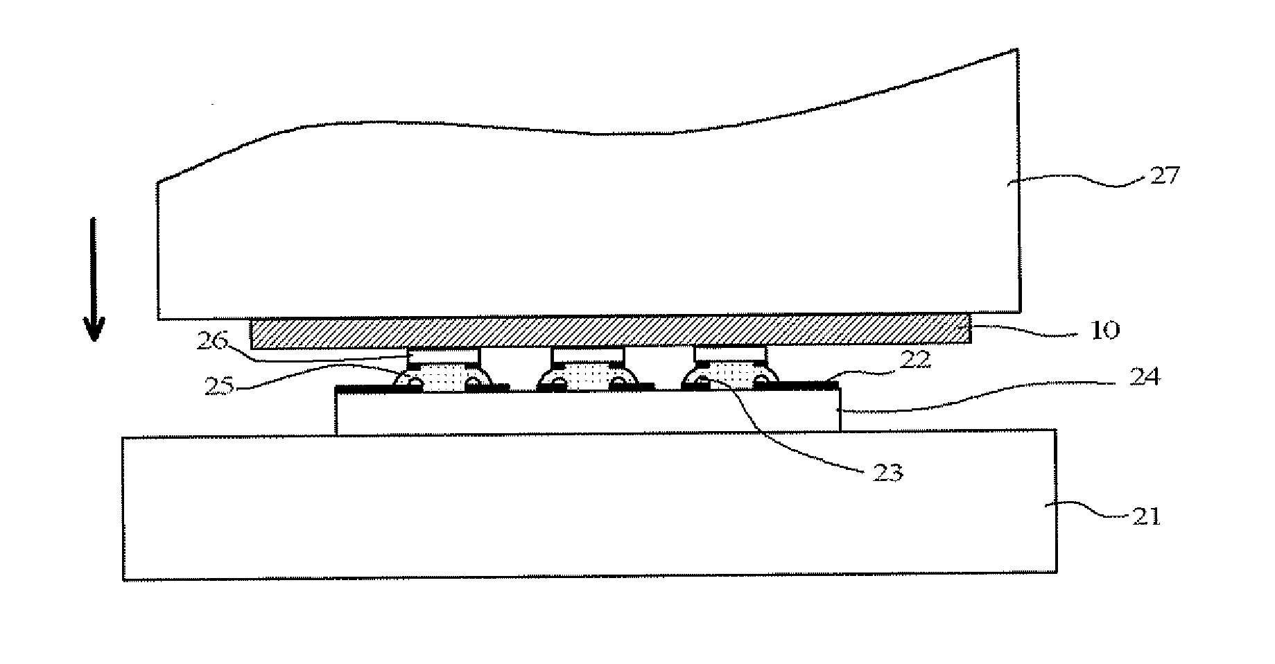
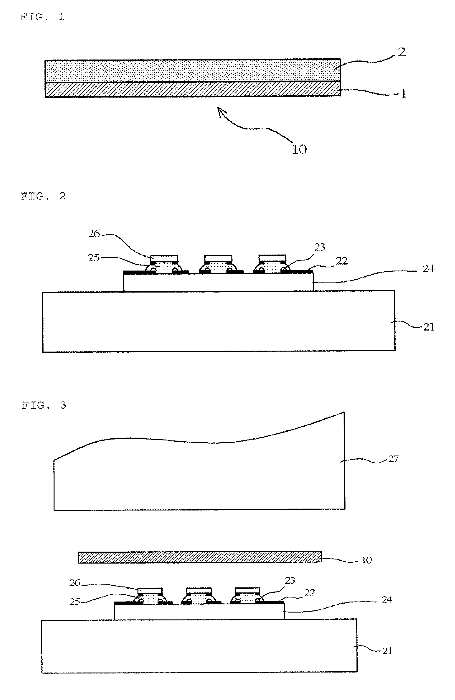
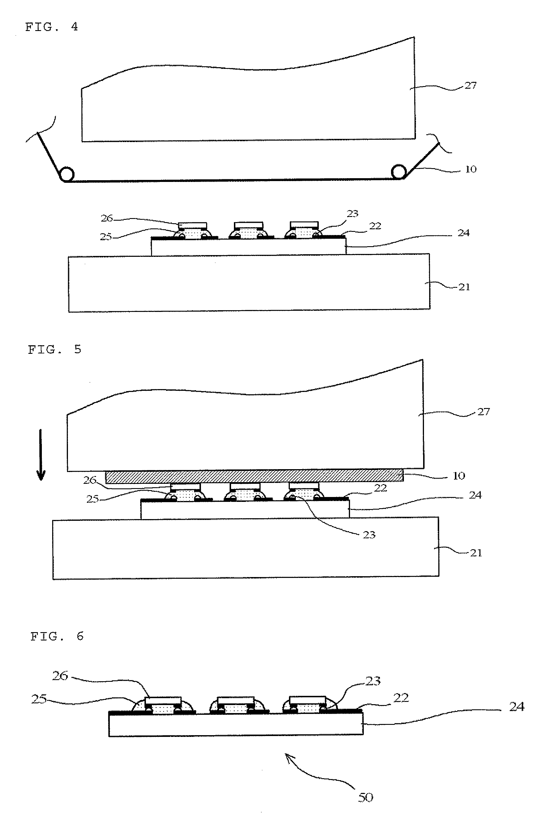
A buffer film for multi-chip packaging which does not cause out of alignment during multi-chip packaging and ensures favorable connection reliability has a structure in which a heat-resistant resin layer having a linear expansion coefficient of 80 ppm / ° C. or less and a flexible resin layer made of a resin material having a Shore A hardness according to JIS K6253 of 10 to 80 are laminated. A multi-chip module can be produced by aligning a plurality of chip devices on a substrate through an adhesive to perform temporary adhesion, disposing the buffer film for multi-chip packaging between the chip devices and a bonding head so that the heat-resistant resin layer is on a chip device side, and connecting the plurality of chip devices with the substrate by applying heat and pressure to the chip devices toward the substrate with the bonding head.
Description
TECHNICAL FIELD[0001]The present invention relates to a buffer film for multi-chip packaging and a method for producing a multi-chip module using the same.BACKGROUND ART[0002]Hitherto, a plurality of chip devices such as LED devices are collectively connected with a substrate through a non-conductive adhesive or an anisotropic conductive adhesive by applying heat and pressure with a bonding head. However, there are difference or variation of height of the chip devices and difference or variation of thickness of wirings or height of bumps formed on the chip device or the substrate. Therefore, the heat and pressure applied to each chip device are different. As a result, a chip device not to be heated and pressurized sufficiently or a chip device to be heated and pressurized excessively may be produced. In the former case, connection failure may occur, and in the latter case, the chip device may be damaged.[0003]In order to eliminate the difference or variation of height of the chip de...
Claims
Login to View More Application Information
Patent Timeline
 Patent Type & Authority Patents(United States)
IPC IPC(8): H01L21/00
CPCH01L2224/7532H01L2924/01006H01L2924/01004H01L24/32H01L2224/75315C08L79/08H01L2224/29387H01L24/95C08L27/06H01L33/005H01L2224/29101H01L2924/01047H01L2924/07811H01L2924/01079H01L2924/01013H01L2224/81001H01L2224/83192H01L2224/29364H01L2224/29324H01L2224/29355C08L67/00H01L24/83H01L2224/81444H01L2224/29339H01L2224/16225H01L2224/13144H01L24/75H01L2224/131H01L2924/12041H01L24/29H01L2224/83907H01L2224/2939H01L2224/29347H01L2933/0066H01L2224/9205H01L24/81H01L2224/81203H01L2224/9211H01L33/48H01L24/92H01L2224/2929H01L2224/29344H01L2224/75985H01L2224/73204H01L2924/01033H01L2924/01005H01L2224/294H01L2924/01019H01L2224/73104H01L24/16H01L2224/32225H01L2924/014H01L25/0753H01L2224/83851H01L2224/83203H01L2224/8385H01L2924/01023H01L2224/92143H01L2224/2919H01L2224/7598H01L33/60H01L2924/01029C08L83/04H01L2224/293H01L2224/81192H01L2924/0665H01L2924/0103H01L2224/81193H01L2924/07802H01L2924/15787H01L2924/15788Y10T156/10Y10T428/24967Y10T428/31544Y10T428/31663H01L2224/75317H01L33/62H01L2933/0033B32B7/12B32B27/08B32B27/281B32B27/283B32B27/304B32B27/32B32B27/36B32B2307/306B32B2307/416B32B2307/536B32B2457/00H01L2224/75314H01L2224/97H01L2924/00014H01L2224/81H01L2224/83H01L2924/00012H01L2924/00H01L2924/3512H01L33/56
Inventor ISHIGAMI, AKIRAKANISAWA, SHIYUKINAMIKI, HIDETSUGUUMAKOSHI, HIDEAKIAOKI, MASAHARU
Owner DEXERIALS CORP
Features
- R&D
- Intellectual Property
- Life Sciences
- Materials
- Tech Scout
- Unparalleled Data Quality
- Higher Quality Content
- 60% Fewer Hallucinations
Learn More Browse by: Latest US Patents, China's latest patents, Technical Efficacy Thesaurus, Application Domain, Technology Topic, Popular Technical Reports.
© 2025 PatSnap. All rights reserved.Legal|Privacy policy|Modern Slavery Act Transparency Statement|Sitemap|About US| Contact US: help@patsnap.com