Wavelength conversion element including phosphor particles, and LED element and semiconductor laser light emitting device using wavelength conversion element
a technology of wavelength conversion element and phosphor particle, which is applied in semiconductor lasers, lighting and heating apparatus, instruments, etc., can solve the problems of reducing the amount of light output from the white led element, reducing the balance between light emitted from the led chip and light emitted from the phosphor, and reducing the amount of light output from the led chip. , to achieve the effect of adjusting the chromaticity of emitted light with more eas
- Summary
- Abstract
- Description
- Claims
- Application Information
AI Technical Summary
Benefits of technology
Problems solved by technology
Method used
Image
Examples
embodiment 1
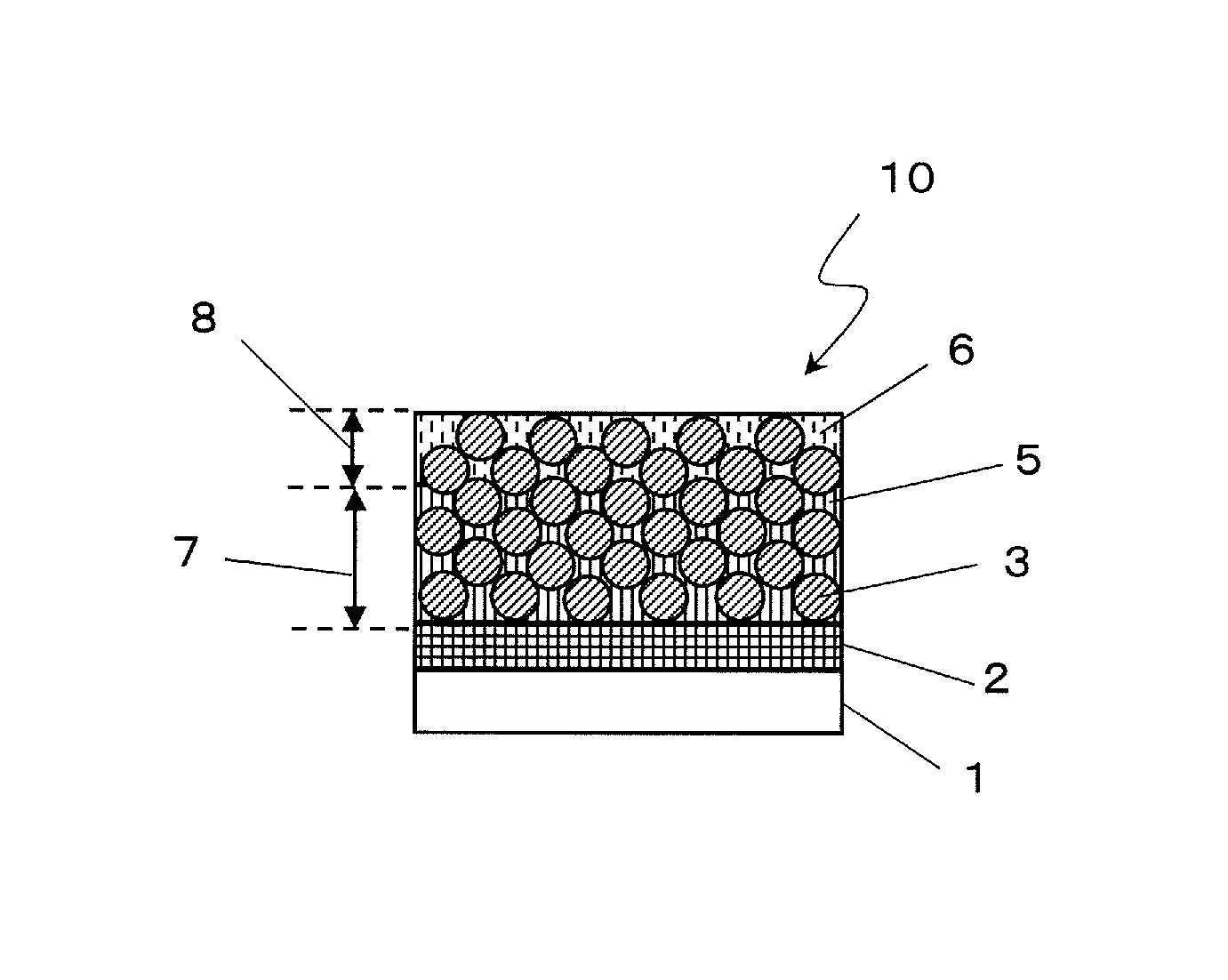
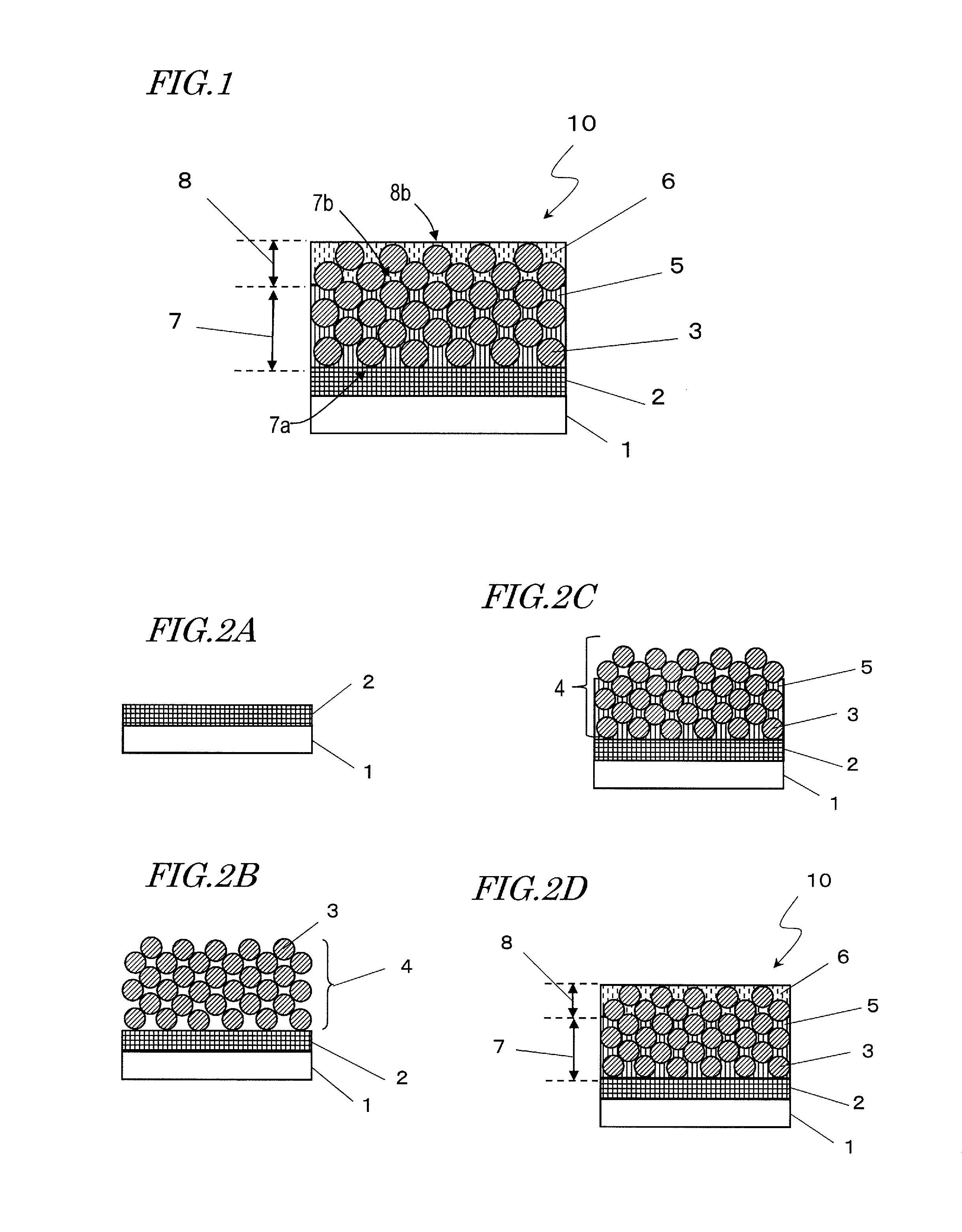
[0092]FIG. 1 is a sectional view of a wavelength conversion element of Embodiment 1.
[0093]A wavelength conversion element 10 according to this embodiment includes a first phosphor layer 7 and a second phosphor layer 8. The wavelength conversion element 10 converts at least a part of incident light into light in a wavelength band which is different from the wavelength band of the incident light and emits the converted light.
[0094]The first phosphor layer 7 includes a part of a plurality of phosphor particles 3 and a first matrix 5 located among the part of the plurality of phosphor particles 3 and formed of zinc oxide in a c-axis orientation. The second phosphor layer 8 includes the remaining part of the plurality of phosphor particles 3 and a second matrix 6 located among the remaining part of the plurality of phosphor particles 3 and formed of a material having a refractive index which is lower than that of zinc oxide. Specifically, in the wavelength conversion element 10, a part o...
embodiment 2
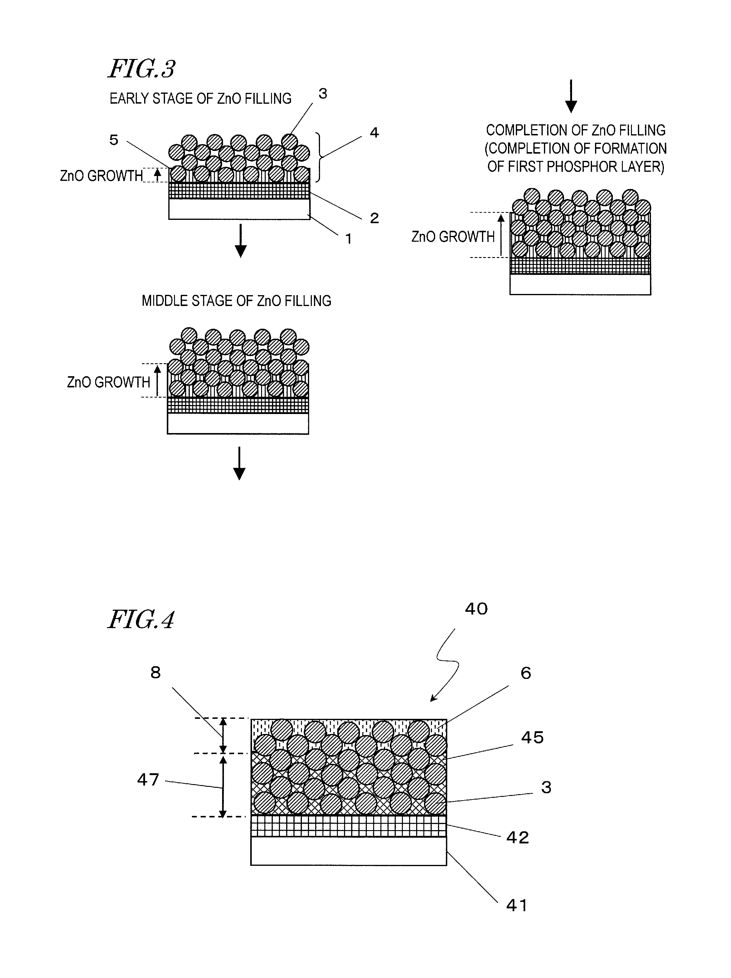
[0127]FIG. 4 is a sectional view of a wavelength conversion element according to Embodiment 2. A wavelength conversion element 40 according to this embodiment includes a substrate 41, a thin film 42, a first phosphor layer 47, and the second phosphor layer 8. The first phosphor layer 47 includes a part of the plurality of phosphor particles 3 and a first matrix 45 located thereamong. The first matrix 45 is formed of single crystalline zinc oxide. Further, the substrate 41 is a single crystalline substrate, and the thin film 42 is formed of single crystalline zinc oxide. The second phosphor layer 8 is the same as the second phosphor layer 8 of Embodiment 1.
[0128]In Embodiment 2, a part of the spaces in the phosphor particle layer 4 which is formed of the phosphor particles 3 is filled with single crystalline zinc oxide which is epitaxially grown from the thin film 42 of single crystalline zinc oxide, and the remaining part of the spaces is filled with a material having a refractive i...
embodiment 3
[0137]An LED element according to an embodiment of the present invention is described.
[0138]The LED element according to this embodiment can use any one of the wavelength conversion elements according to Embodiments 1 and 2. FIG. 6A illustrates the wavelength conversion element 10 described in Embodiment 1 in a state of being upside down.
[0139]FIG. 6B is a sectional view of the LED element according to Embodiment 3. Electrodes of the LED chip, the internal structure of the LED chip, and the like are simplified for the sake of easy understanding. As illustrated in FIG. 6B, an LED element 60 includes a support 61, an LED chip 62, and a wavelength conversion element 50. As described above, as the wavelength conversion element 50, the wavelength conversion element 10 described in Embodiment 1 or the wavelength conversion element 40 described in Embodiment 2 is used.
[0140]The support 61 supports the LED chip 62. In this embodiment, the LED element 60 has a structure which enables surface...
PUM
 Abstract
Description
Claims
Application Information


