Method of making highly-confined semiconductor nanocrystals

a nanocrystal and high-confined technology, applied in the direction of oxide conductors, non-metal conductors, conductors, etc., can solve the problems of thermal quenching of quantum efficiency, poor temperature stability, and difficulty in tuning the emission response, and achieve good quantum efficiencies, high confinement, and good quantum efficiencies

Active Publication Date: 2014-07-22
NANOCO TECH LTD
View PDF12 Cites 6 Cited by
  • Summary
  • Abstract
  • Description
  • Claims
  • Application Information

AI Technical Summary

Benefits of technology

[0014]It is an advantage of the present invention that the high confinement semiconductor nanocrystals formed in accordance with the present invention exhibit the desirable properties of good quantum efficiencies (>70%) at room temperature and maintain these good quantum efficiencies at elevated temperatures (up to temperatures of ˜175° C.). It is also an advantage that the electron-phonon interaction is reduced in these nanocrystals. Another benefit of the present invention is that high confinement semiconductor nanocrystals exhibiting these properties can be used to create advantaged quantum dot phosphors, high intensity LEDs, and both optically and electrically pumped lasers.
that the high confinement semiconductor nanocrystals formed in accordance with the present invention exhibit the desirable properties of good quantum efficiencies (>70%) at room temperature and maintain these good quantum efficiencies at elevated temperatures (up to temperatures of ˜175° C.). It is also an advantage that the electron-phonon interaction is reduced in these nanocrystals. Another benefit of the present invention is that high confinement semiconductor nanocrystals exhibiting these properties can be used to create advantaged quantum dot phosphors, high intensity LEDs, and both optically and electrically pumped lasers.

Problems solved by technology

Despite the very good quantum efficiencies of conventional phosphors, they suffer from enhanced optical backscattering due to their large size and it is difficult to tune their emission response in order to get spectra with specific correlated color temperatures (CCT) having high color rendering index (CRI) values.
Despite these advantages, colloidal quantum dot phosphors have not been introduced into the marketplace due to two major shortcomings; namely, poor temperature stability (thermal quenching of quantum efficiency) (N. Pradhan et al., J. Am. Chem. Soc. 127 (50), 17586 (2005)) and low (10-20%) quantum yields for phosphor films with high quantum dot packing densities.
One way to get around the non-ideal temperature stability of colloidal quantum dots is to dope the nanocrystals with impurity atoms, as was done by Peng and co-workers (N. Pradhan et al., J. Amer. Chem. Soc. 129, 3339 (2007)), where it was found that Mn-doped ZnSe nanocrystals maintained a reasonable thermal stability up to ˜250° C. The disadvantages of this approach are that the peak emission wavelengths of the nanocrystals are limited by the particular choice of dopant materials, the spectral widths of the photoluminescence are typically larger for impurity emission, and the quantum efficiency of these types of nanocrystals is below that of undoped nanocrystals.
The problems with this approach are that the shell growth times can be prohibitively long and the quantum efficiency tends to fall for very thick shells due to their greater propensity for defect formation.
To date, traditional (not employing impurity dopants) nanocrystals suffer from poor thermal stability which limits the usefulness of these materials in high temperature applications, such as, high power LEDs and nanocrystal-based lasers.
However, the engineered nanocrystals had other problems, such as, reduced quantum efficiencies at room temperature.

Method used


Image

  • Method of making highly-confined semiconductor nanocrystals
  • Method of making highly-confined semiconductor nanocrystals
  • Method of making highly-confined semiconductor nanocrystals

Examples


example i-1

Preparation of the Inventive Shelled High Confinement Semiconductor Nanocrystals, InP / InGaP / ZnSe / ZnSeS / ZnS

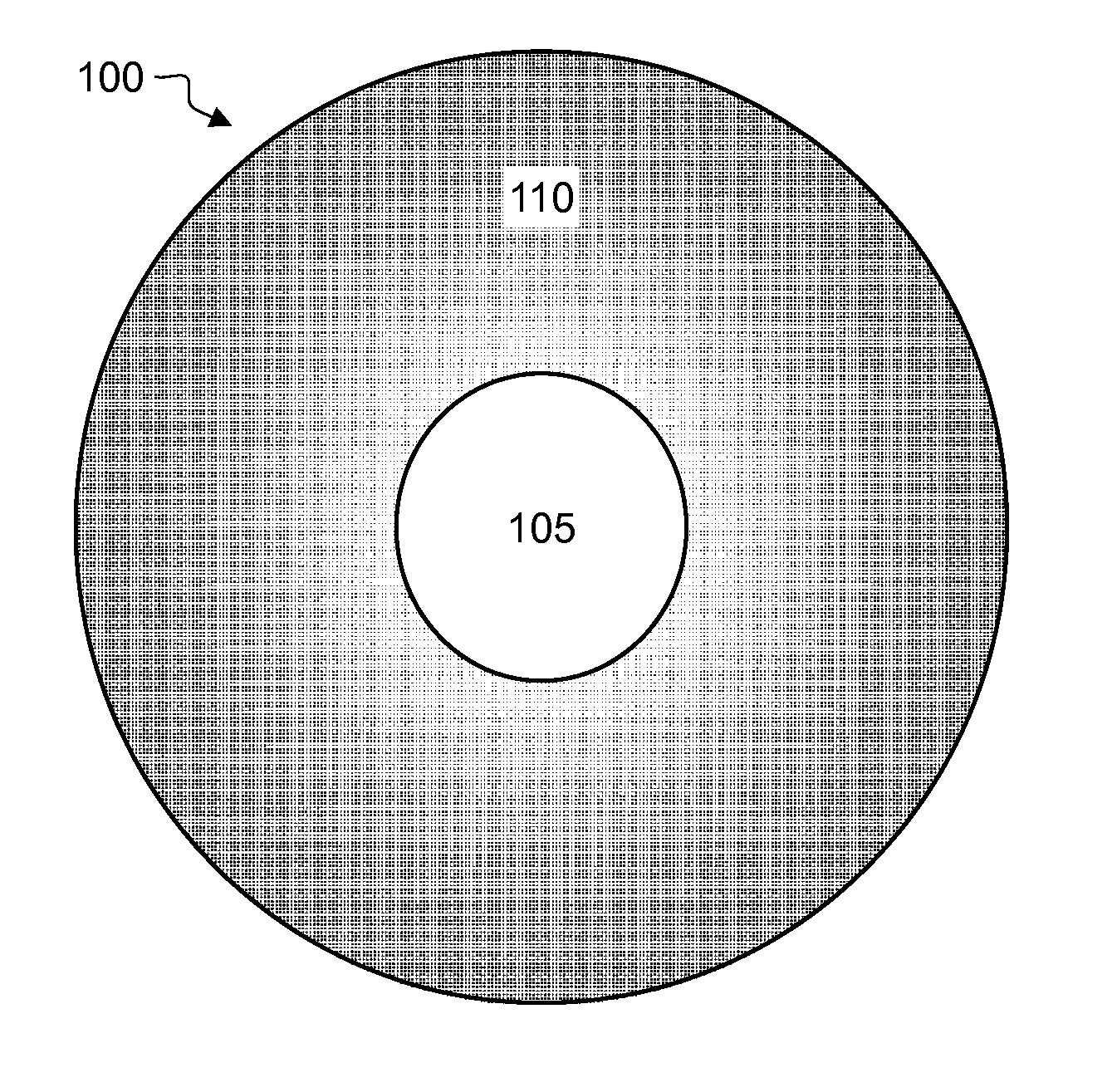
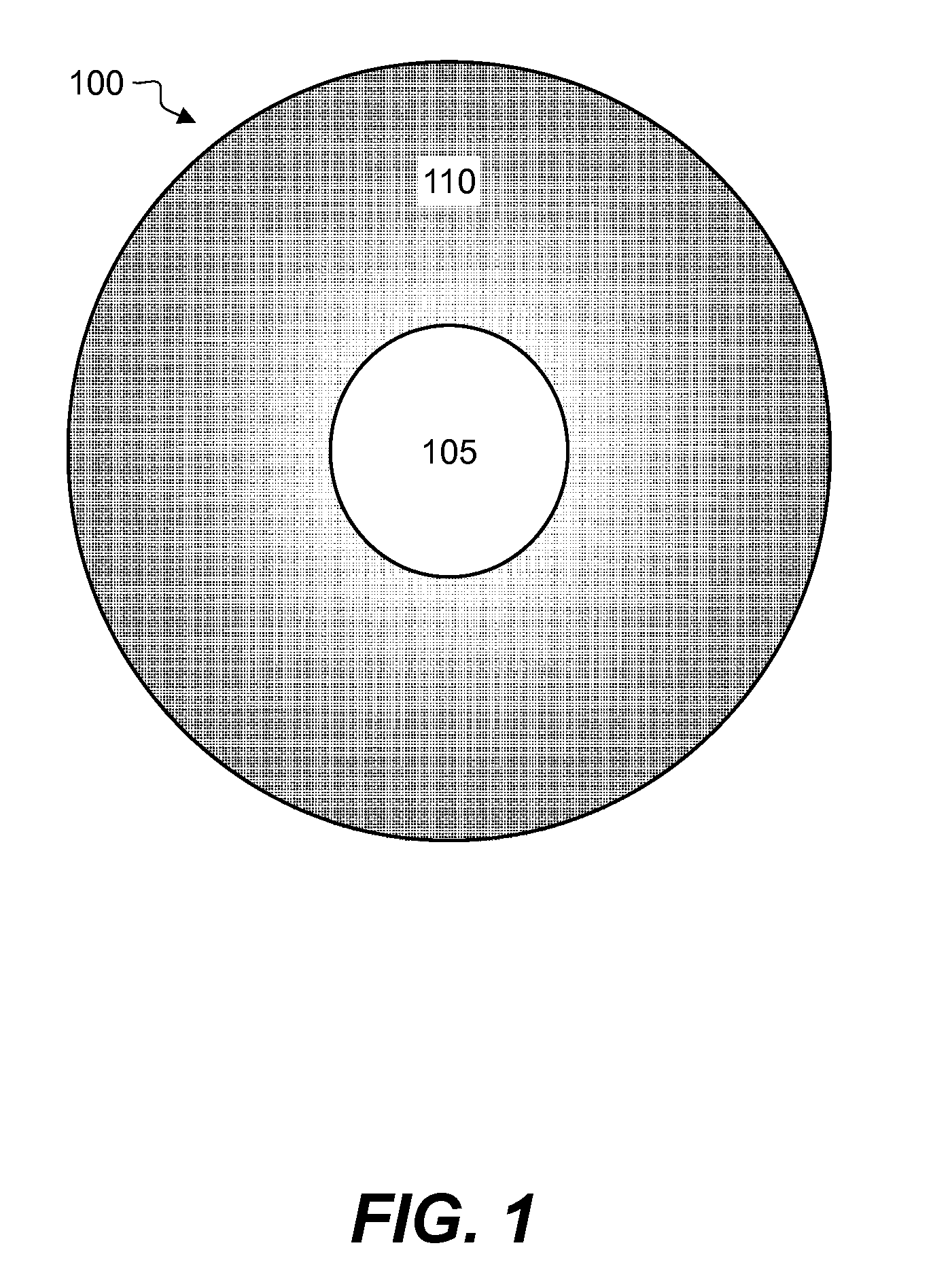
[0037]All synthetic routes were carried out using standard airless procedures with a dry box and a Schlenk line. In one growth step both the compact homogenous semiconductor region 105, composed of InP, and the gradient alloy region 110, composed of InGaP, are formed. 0.12 g (0.52 mmol) myristic acid, 0.045 g (0.1 mmol) Zn undecylenate and 7 ml 1-octadecene (ODE) were loaded into a three neck flask. The mixture was degassed at 100° C. for 1 hour. After switching to N2 overpressure, the flask contents were heated to 300° C., while vigorously stirring its contents. Two precursor solutions were prepared and loaded into corresponding syringes. The first precursor solution contained 0.013 g (0.08 mmol) trimethylindium (In(Me)3), 0.012 g (0.048 mmol) tris(trimethylsilyl)phosphine (P(TMS)3), 0.08 mmol oleylamine and 2 ml ODE; the second precursor solution contained 0.013 g (0.08 mmol) ...

example i-2

Preparation of the Inventive Shelled High Confinement Semiconductor Nanocrystals, InP / InGaP / ZnSe / ZnSeS

[0041]All synthetic routes were carried out using standard airless procedures with a dry box and a Schlenk line. In one growth step both the compact homogenous semiconductor region 105, composed of InP, and the gradient alloy region 110, composed of InGaP, are formed. 0.12 g (0.52 mmol) myristic acid, 0.045 g (0.1 mmol) Zn undecylenate and 7 ml ODE were loaded into a three neck flask. The mixture was degassed at 100° C. for 1 hour. After switching to N2 overpressure, the flask contents were heated to 300° C., while vigorously stirring its contents. Two precursor solutions were prepared and loaded into corresponding syringes. The first precursor solution contained 0.013 g (0.08 mmol) trimethylindium, 0.012 g (0.048 mmol) tris(trimethylsilyl)phosphine, 0.08 mmol oleylamine and 2 ml ODE; the second precursor solution contained 0.013 g (0.08 mmol) triethylgallium, 0.08 mmol oleylamine a...

example i-3

Preparation of Prior Art Shelled InP-Based Nanocrystals, InP / ZnSe / ZnSeS

[0045]The InP cores were formed by the following process. 0.12 g (0.52 mmol) myristic acid, 0.045 g (0.1 mmol) Zn undecylenate and 7 ml ODE were loaded into a three neck flask. The mixture was degassed at 100° C. for 1 hour. After switching to N2 overpressure, the flask contents were heated to 300° C., while vigorously stirring its contents. Two precursor solutions were prepared and loaded into corresponding syringes. The first precursor solution contained 0.013 g (0.08 mmol) trimethylindium, 0.012 g (0.048 mmol) tris(trimethylsilyl)phosphine, 0.08 mmol oleylamine and 2 ml ODE; the second precursor solution contained 0.013 g (0.08 mmol) trimethylindium, 0.08 mmol oleylamine and 1.5 ml ODE. When the reaction flask reached 300° C., the first syringe was quickly injected into the hot flask. After a time delay of 0.5 to 1.0 s, the second syringe was rapidly injected into the hot flask. After the second injection, the...


PUM

PropertyMeasurementUnit
temperatureaaaaaaaaaa
quantum efficiencyaaaaaaaaaa
diameteraaaaaaaaaa

Abstract

A method of making a colloidal solution of high confinement semiconductor nanocrystals includes: forming a first solution by combining a solvent, growth ligands, and at most one semiconductor precursor; heating the first solution to the nucleation temperature; and adding to the first solution, a second solution having a solvent, growth ligands, and at least one additional and different precursor than that in the first solution to form a crude solution of nanocrystals having a compact homogenous semiconductor region. The method further includes: waiting 0.5 to 20 seconds and adding to the crude solution a third solution having a solvent, growth ligands, and at least one additional and different precursor than those in the first and second solutions; and lowering the growth temperature to enable the formation of a gradient alloy region around the compact homogenous semiconductor region, resulting in the formation of a colloidal solution of high confinement semiconductor nanocrystals.

Description

STATEMENT REGARDING FEDERALLY-SPONSORED RESEARCH OR DEVELOPMENT[0001]This invention was made with Government support under Cooperative Agreement #DE-EE000979 awarded by DOE. The Government has certain rights in this invention.CROSS-REFERENCE TO RELATED APPLICATIONS[0002]Reference is made to commonly assigned U.S. patent application Ser. No. 13 / 024,555 filed Feb. 10, 2011, entitled “Indium Phosphide Colloidal Nanocrystals” by Xiaofen Ren et al, and U.S. patent application Ser. No. 13 / 275,424 filed Oct. 18, 2011, entitled “Highly-Confined Semiconductor Nanocrystals” by Keith B. Kahen et al, the disclosures of which are incorporated herein.FIELD OF THE INVENTION[0003]The present invention relates to forming nanocrystals, wherein the inner homogenous region of the core is highly confined.BACKGROUND OF THE INVENTION[0004]For solid-state lighting applications, the fastest route to high efficiency white LEDs is to combine either blue, violet, or near UV LEDs with appropriate phosphors. The...

Claims


Application Information

Patent Timeline
Patent Type & Authority Patents(United States)
IPC IPC(8): H01B1/06
CPCC09K11/02C09K11/565C09K11/70C09K11/883H01L33/502
Inventor KAHEN, KEITH BRIANHOLLAND, MATTHEWPALLIKKARA KUTTIATOOR, SUDEEP
Owner NANOCO TECH LTD
Why Eureka
Try Eureka