Silicon carbide semiconductor device

a technology of silicon carbide and semiconductors, applied in the direction of semiconductor devices, basic electric elements, electrical equipment, etc., can solve the problems of high resistance of mosfet, inability to achieve inability to improve breakdown voltage by making full use of sic physical properties advantages, etc., to achieve the ratio of voltage across the first and second electrodes, the effect of reducing the depth of the relaxing region and reducing the electric field intensity

Active Publication Date: 2014-08-12
SUMITOMO ELECTRIC IND LTD
View PDF7 Cites 0 Cited by
  • Summary
  • Abstract
  • Description
  • Claims
  • Application Information

AI Technical Summary

Benefits of technology

[0010]According to the silicon carbide semiconductor device above, the impurity dose amount in the relaxing region is increased to satisfy relation of Drx>Ld·Nd. Thus, when a voltage across the first and second electrodes becomes higher as the silicon carbide semiconductor device is set to an OFF state, the relaxing region is prevented from being completely depleted before a depletion layer sufficiently extends from the relaxing region to the first main surface of the silicon carbide layer. Thus, the depletion layer having a sufficient length can be formed between the relaxing region and the first main surface. Therefore, a ratio of a voltage across the first and second electrodes borne by a portion between the relaxing region and the first main surface is increased. In other words, a voltage borne by a portion shallower than the relaxing region is mitigated. Thus, electric field intensity in a portion shallower than the relaxing region can be lessened. In other words, electric field intensity in a portion where breakdown is likely due to electric field concentration can be lessened. Thus, a higher voltage can be applied across the first and second electrodes without causing breakdown. Namely, a breakdown voltage of the silicon carbide semiconductor device is raised.
[0011]Preferably, relation of Ld≧5 μm is satisfied. Thus, a depletion layer having a length of 5 μm at the maximum can be formed between the relaxing region and the first main surface. In other words, a depletion layer having a sufficient length can more reliably be formed between the relaxing region and the first main surface. Therefore, a breakdown voltage of the silicon carbide semiconductor device can further be raised.
[0012]Preferably, relation of Drx≧1×1013 cm−2 is satisfied. Thus, when a voltage across the first and second electrodes is raised as the silicon carbide semiconductor device is set to the OFF state, the relaxing region is prevented from being completely depleted before a depletion layer sufficiently extends from the relaxing region to the first main surface of the silicon carbide layer. Therefore, a breakdown voltage of the silicon carbide semiconductor device can further be raised.
[0014]Preferably, the silicon carbide semiconductor device has a single crystal substrate. The single crystal substrate is provided between the first main surface of the silicon carbide layer and the first electrode, is in contact with each of the first main surface of the silicon carbide layer and the first electrode, is composed of silicon carbide, has the first conductivity type, and has an impurity concentration higher than impurity concentration Nd. Thus, the drift layer and the first electrode are connected to each other with a single crystal substrate having an impurity concentration higher than impurity concentration Nd being interposed. Therefore, contact resistance of the first electrode can be lower. Therefore, electrical resistance of the drift layer can accordingly be higher.
[0016]Preferably, a distance Ltr between the relaxing region and the bottom surface of the trench is not greater than 4 μm. Thus, electric field concentration at the gate insulating film on the bottom surface of the trench can more effectively be suppressed. Therefore, a breakdown voltage of the silicon carbide semiconductor device can further be raised.
[0018]Preferably, the body region is a well region having a side surface and a bottom surface as well as a corner portion between the side surface and the bottom surface. A distance Lpn between the relaxing region and the corner portion of the well region is not greater than 4 μm. Thus, electric field concentration at the corner portion of the well region where breakdown is particularly likely can be suppressed. Therefore, a breakdown voltage of the silicon carbide semiconductor device can further be raised.

Problems solved by technology

This method, however, is disadvantageous in high ON resistance of a MOSFET.
In a case where such high electric field may be applied, breakdown due to electric field concentration at a specific position in a MOSFET structure gives rise to a problem.
Therefore, if the technique in the document above which is considered to be premised on use of Si is simply applied for improvement of a breakdown voltage of an SiC semiconductor device, improvement in breakdown voltage by making full use of advantages in terms of physical properties of SiC cannot be achieved.

Method used


Image

  • Silicon carbide semiconductor device
  • Silicon carbide semiconductor device
  • Silicon carbide semiconductor device

Examples


first embodiment

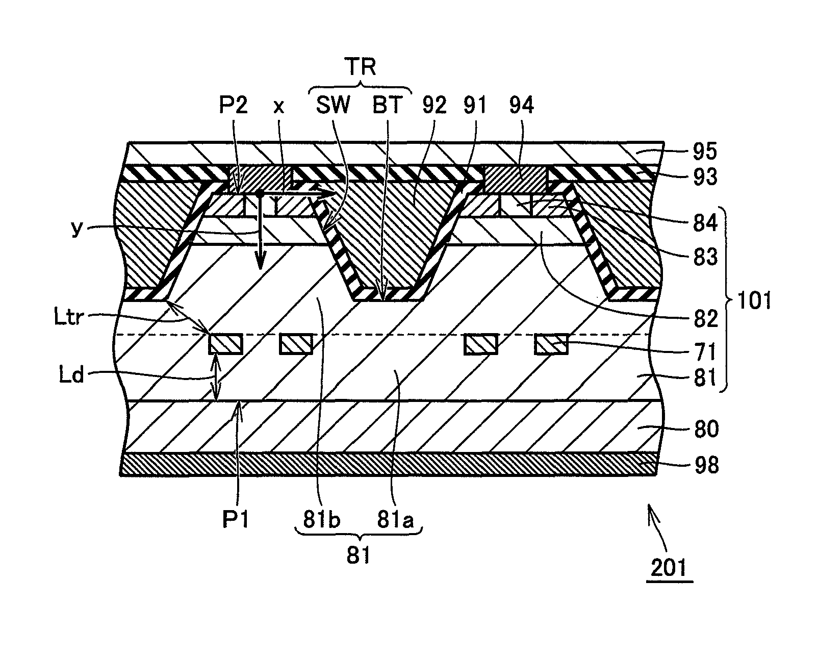
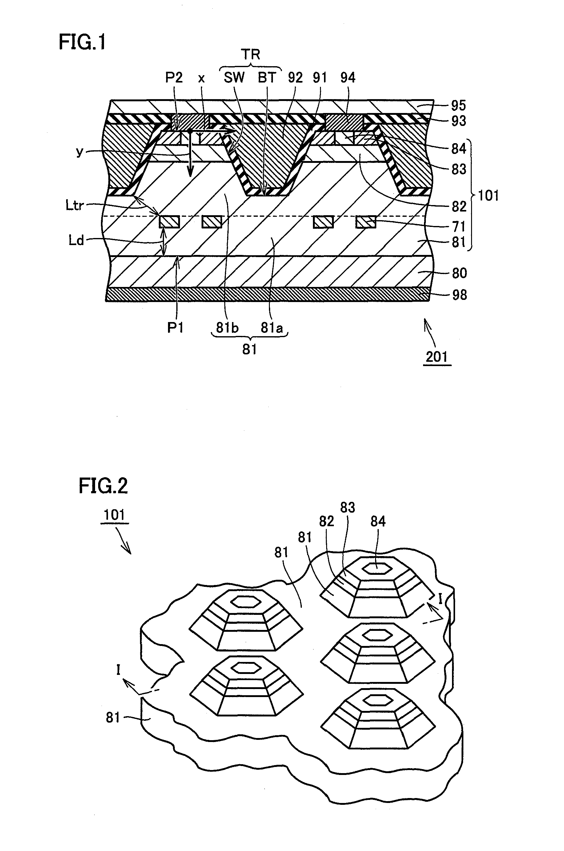
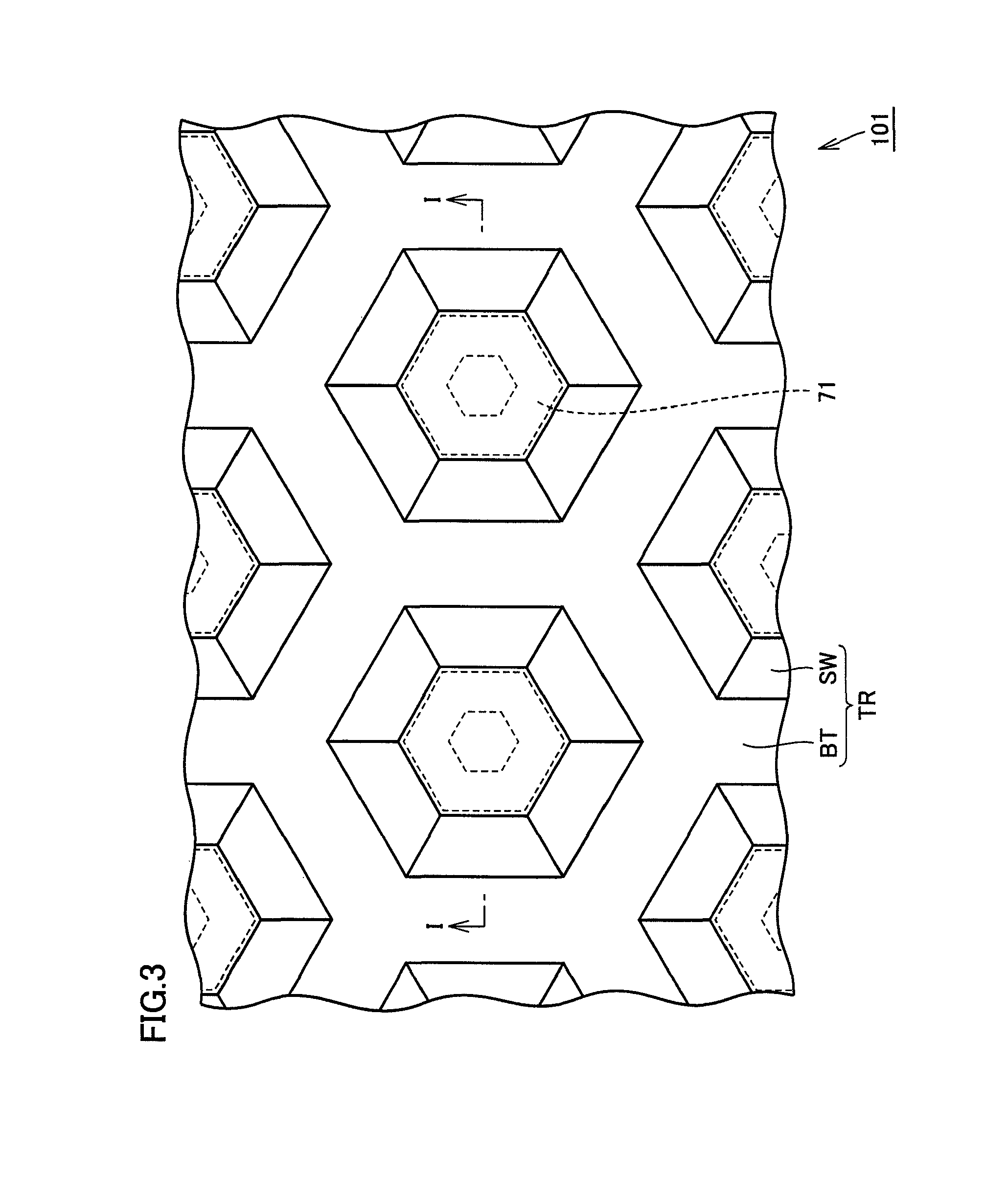
[0068]As shown in FIGS. 1 to 3, a MOSFET 201 (a silicon carbide semiconductor device) in the present embodiment has a single crystal substrate 80, an epitaxial layer 101 (a silicon carbide layer), a gate oxide film 91 (a gate insulating film), a gate electrode 92, an interlayer insulating film 93, a source electrode 94 (a second electrode), a source interconnection layer 95, and a drain electrode 98 (a first electrode). MOSFET 201 preferably has a breakdown voltage not lower than 600 V across drain electrode 98 and source electrode 94. In other words, MOSFET 201 is preferably a power semiconductor device having a high breakdown voltage.

[0069]Epitaxial layer 101 is a silicon carbide layer epitaxially grown on single crystal substrate 80. Epitaxial layer 101 has hexagonal crystal structure having a poly type of 4H. Epitaxial layer 101 has a lower surface P1 (a first main surface) facing single crystal substrate 80 and an upper surface P2 (a second main surface) opposite to lower surfa...

second embodiment

[0113]Referring to FIG. 17, a MOSFET 202 in the present embodiment has an epitaxial layer 102 instead of epitaxial layer 101 in the first embodiment. Epitaxial layer 102 has a relaxing region 72. Relaxing region 72 has a shape from which an opening in relaxing region 71 (FIG. 3) has been eliminated in a plan view (FIG. 18). Namely, relaxing region 72 has a shape similar to the hexagonal shape of upper surface P2 in a plan view. It is noted that features other than the above are substantially the same as those in the first embodiment described above, and therefore the same or corresponding elements have the same reference characters allotted and description thereof will not be repeated.

third embodiment

[0114]Referring to FIG. 19, a MOSFET 203 in the present embodiment has an epitaxial layer 103 instead of epitaxial layer 101 in the first embodiment. Epitaxial layer 103 has a relaxing region 73. Relaxing region 73 extends along trench TR in a plan view (FIG. 20). It is noted that features other than the above are substantially the same as those in the first embodiment described above, and therefore the same or corresponding elements have the same reference characters allotted and description thereof will not be repeated.

[0115]Then, intensity of electric field in a direction of thickness (a vertical direction in FIG. 19) applied to gate oxide film 91 at a position lying between n drift layer 81 and the corner portion of trench TR while MOSFET 203 is in the OFF state (hereinafter referred to as corner portion electric field intensity) was simulated. Consequently, corner portion electric field intensity of MOSFET 203 having relaxing region 73 was 5.7 MV / cm. In contrast, in a comparati...


PUM


Abstract

A drift layer forms a first main surface of a silicon carbide layer and has a first conductivity type. A source region is provided to be spaced apart from the drift layer by a body region, forms a second main surface, and has the first conductivity type. A relaxing region is provided within the drift layer and has a distance Ld from the first main surface. The relaxing region has a second conductivity type and has an impurity dose amount Drx. The drift layer has an impurity concentration Nd between the first main surface and the relaxing region. Relation of Drx>Ld·Nd is satisfied. Thus, a silicon carbide semiconductor device having a high breakdown voltage is provided.

Description

BACKGROUND OF THE INVENTION[0001]1. Field of the Invention[0002]This invention relates to a silicon carbide semiconductor device and particularly to a silicon carbide semiconductor device having a gate insulating film and a method for manufacturing the same.[0003]2. Description of the Background Art[0004]In an Si (silicon) MOSFET (Metal Oxide Semiconductor Field Effect Transistor) representing a widely used power semiconductor device, a main factor determining a breakdown voltage is an upper limit of electric field intensity which a drift layer forming a breakdown voltage holding region can withstand. A drift layer made of Si may break down at a portion where electric field not lower than approximately 0.3 MV / cm is applied. Therefore, it is necessary to suppress electric field intensity to be less than a prescribed value in the entire drift layer of a MOSFET. The simplest method is to lower an impurity concentration in a drift layer. This method, however, is disadvantageous in high ...

Claims


Application Information

Patent Timeline
Patent Type & Authority Patents(United States)
IPC IPC(8): H01L29/66
CPCH01L29/7802H01L29/66068H01L29/4238H01L29/0623H01L29/4236H01L29/0696H01L21/0475H01L29/1608H01L29/7813H01L29/045H01L21/3065
Inventor WADA, KEIJIMASUDA, TAKEYOSHIHIYOSHI, TORU
Owner SUMITOMO ELECTRIC IND LTD
Why Eureka
Try Eureka