Cross-interference reduction of a buck power converter

a cross-interference reduction and power converter technology, applied in the direction of electric variable regulation, process and machine control, instruments, etc., can solve problems such as not cost-efficien

Active Publication Date: 2014-08-12
RICHTEK TECH
View PDF5 Cites 22 Cited by
  • Summary
  • Abstract
  • Description
  • Claims
  • Application Information

AI Technical Summary

Problems solved by technology

However, the two-step power converter 22 induces new problems, specifically the cross-interference between the voltages at different voltage outputs Vout1, Vout2 and Vout3.
However, it is not cost-efficient because the output voltage of the first conversion stage of the power converter is wasted.

Method used


Image

  • Cross-interference reduction of a buck power converter
  • Cross-interference reduction of a buck power converter
  • Cross-interference reduction of a buck power converter

Examples


first embodiment

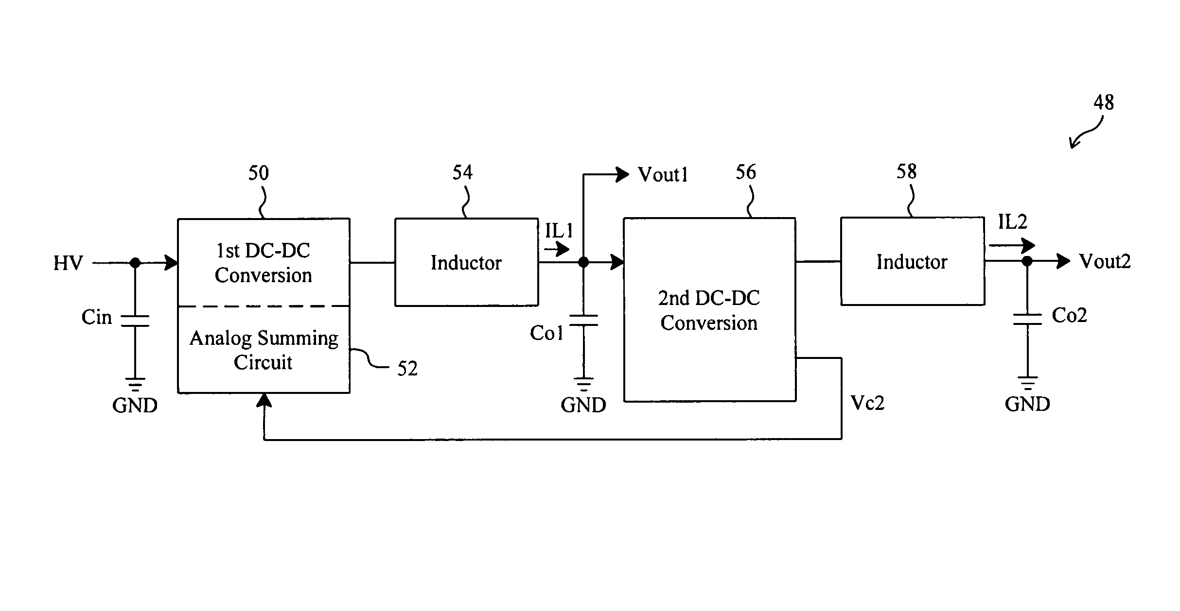
[0023] as shown in FIG. 6, a two-step power converter 48 includes two conversion stages. The first one includes a DC-DC conversion 50 and an inductor 54, and the second one includes a DC-DC conversion 56 and an inductor 58. The first conversion stage converts an input voltage HV to a first output voltage Vout1, and then the second conversion stage converts the first output voltage Vout1 to a second output voltage Vout2. Each of the DC-DC conversions 50 and 56 has one or more pairs of power switches. The DC-DC conversion 56 further includes a PWM control loop for stabling its output voltage Vout2. The PWM control loop for the DC-DC conversion 56 may also refer to FIG. 4. In this case, the error signal Vc2 generated by the PWM control loop for the DC-DC conversion 56 is fed forward to an analog summing circuit 52 of the DC-DC conversion 50, so as to stabilize the output voltage Vout1 of the first conversion stage when the output voltage Vout2 of the second conversion stage varies.

[002...

second embodiment

[0028]FIG. 11 is a circuit diagram of a second embodiment for the analog summing circuit 94 of FIG. 9, in which a PWM comparator 130 having multiple pairs of inputs is used in the PWM control loop of the first conversion stage to produce the PWM signal according to various signals. An error signal Vc1 is generated by an error amplifier 122 according to a reference voltage VREF1 and a feedback signal VFB1 that is derived from and thereby a function of the output voltage Vout1, and sent to a non-inverting input INP1 of the PWM comparator 130. A ramp signal 124 is sent to an inverting input INN1 of the PWM comparator 130. The error signal Vc2 extracted from the DC-DC conversion 96 passes through a high pass filter 126 along with any DC bias VB1 to generate signals Vc2′ and VB1′ (in fact, VB1′=VB1), which are sent to a non-inverting input INP2 and an inverting input INN2 of the PWM comparator 130 respectively. The error signal Vc3 extracted from the DC-DC conversion 98 passes through a ...

third embodiment

[0029]FIG. 12 is a circuit diagram of a third embodiment for the analog summing circuit 94 of FIG. 9, which also uses a PWM comparator 140 having multiple pairs of inputs in the PWM control loop of the first conversion stage for producing the PWM signal. An error signal Vc1 is generated by an error amplifier 132 according to a reference voltage VREF1 and a feedback signal VFB1 that is derived from and thereby a function of the output voltage Vout1, and then sent to a non-inverting input INP1 of the PWM comparator 140. A ramp signal 134 is sent to an inverting input INN1 of the PWM comparator 140. The error signal Vc2 extracted from the DC-DC conversion 96 is sent to a non-inverting input INP2 of the PWM comparator 140. The error signal Vc2 is also filtered by a low pass filter 136 to produce a signal Vc2′ sent to an inverting input INN2 of the PWM comparator 140. The error signal Vc3 extracted from the DC-DC conversion 98 is sent to a non-inverting input INP3 of the PWM comparator 1...


PUM


Abstract

A power converter includes a first conversion stage for converting an input voltage to a first output voltage and a second conversion stage for converting the first output voltage to a second output voltage. An error signal is generated according to a reference voltage and a feedback signal extracted from the second conversion stage, and a feed forward signal is generated from the error signal and injected into the first conversion stage to stabilize the first output voltage. The feedback signal is a function of the second output voltage and thus, the error signal varies with the second output voltage. As a result, the first output voltage will be stabilized when the second output voltage varies, due to the varied feed forward signal.

Description

FIELD OF THE INVENTION[0001]The present invention is related generally to power converters and, more particularly, to cross-interference reduction of a buck power converter.BACKGROUND OF THE INVENTION[0002]FIG. 1 is a diagram showing a conventional buck power converter 10, which has a voltage input Vin to connect with a high voltage, e.g. 12V, and three voltage outputs Vout1, Vout2, and Vout3 to supply low voltages, e.g. 5V, 3.3V, and 1.8V. FIG. 2 is a simplified circuit diagram showing a power conversion stage 12 to convert the input voltage Vin to the output voltage Vout1, which includes a high-side switch 14 and a low-side switch 16 connected in series between a voltage input Vin and a ground terminal GND by a phase node, and an inductor L connected between the phase node and a voltage output Vout1. The power switches 14 and 16 are alternatively switched by pulse width modulation (PWM) signals 18 and 20 respectively, thereby generating a current IL flowing through the inductor L ...

Claims


Application Information

Patent Timeline
Patent Type & Authority Patents(United States)
IPC IPC(8): G05F1/00
CPCH02M2001/007H02M3/1588Y02B70/1466H02M2001/0022Y10T307/406Y02B70/10H02M1/0022H02M1/007
Inventor LIU, JING-MENG
Owner RICHTEK TECH
Why Eureka
Try Eureka