SiGe HBT having deep pseudo buried layer and manufacturing method thereof

a technology of silicongermanium and pseudo-buried layer, which is applied in the direction of basic electric elements, electrical apparatus, and semiconductor devices, can solve the problems of affecting the performance of the device, the inability to adopt an annealing process, etc., and achieves the effect of reducing the current amplification coefficient of a parasitic transistor, reducing the series resistance of the collector region, and reducing the saturation voltage drop of the sige hb

Active Publication Date: 2014-08-26
SHANGHAI HUAHONG GRACE SEMICON MFG CORP
View PDF10 Cites 0 Cited by
  • Summary
  • Abstract
  • Description
  • Claims
  • Application Information

AI Technical Summary

Benefits of technology

[0026]The SiGe HBT having a deep pseudo buried layer of the present invention is capable of reducing the current amplification coefficient of a parasitic transistor consisted of the base region, the collector region and the substrate, of the SiGe HBT, reducing the series resistance of the collector region, and lowering the saturation voltage drop of the SiGe HBT, and thus capable of improving the performance of the device. Moreover, the manufacturing method of the SiGe HBT of the present invention is simple and procedures included therein are reasonably arranged. These features are conductive to facilitate its rapid implementation.

Problems solved by technology

Moreover, it is impractical to adopt an annealing process to realize the lateral connection between the pseudo buried layers 13, as the annealing process will also cause the pseudo buried layers 13 to diffuse toward the surface of the collector region 14 and thus will affect the performance of the device.

Method used


Image

  • SiGe HBT having deep pseudo buried layer and manufacturing method thereof
  • SiGe HBT having deep pseudo buried layer and manufacturing method thereof
  • SiGe HBT having deep pseudo buried layer and manufacturing method thereof

Examples


Embodiment Construction

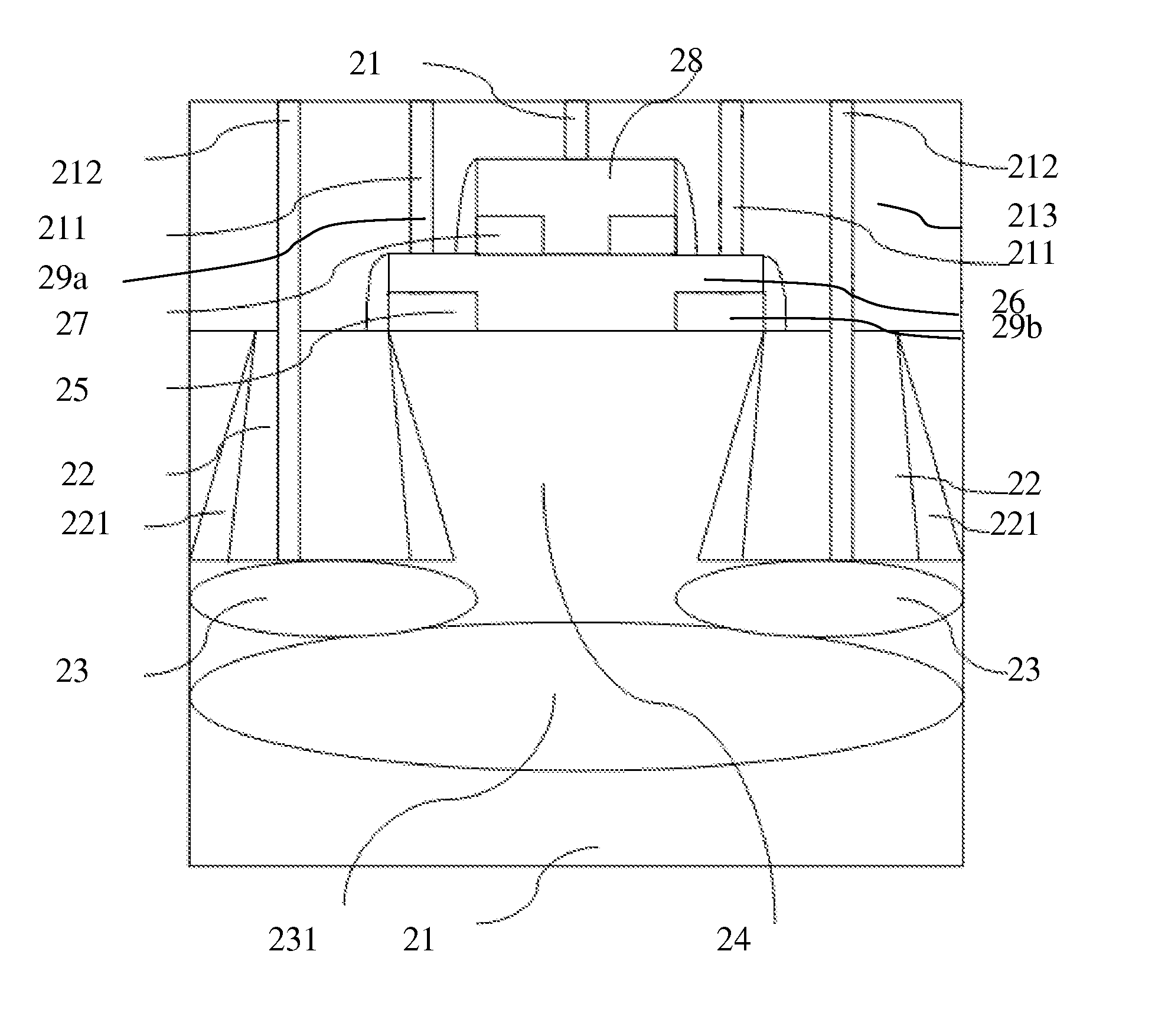
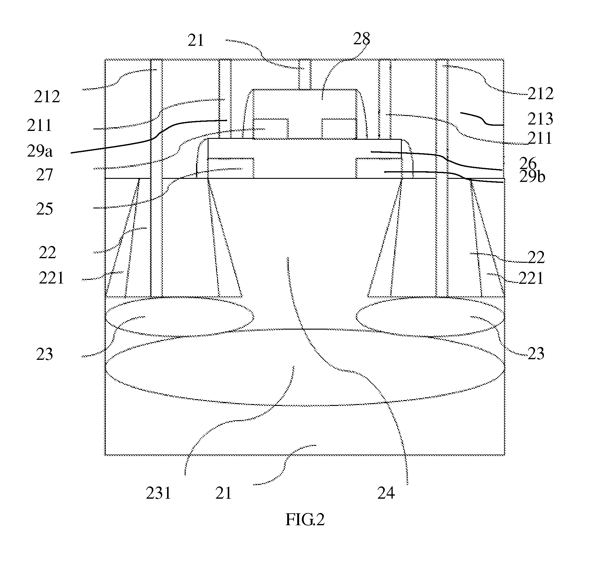
[0030]FIG. 2 illustrates the structure of a silicon-germanium (SiGe) heterojunction bipolar transistor (HBT) constructed according to an embodiment of the present invention. The device has a structure as follows: trenches 22 are formed in a substrate 21; inner sidewalls 221 are formed over inner side faces of each trench 22 and each trench 22 is filled with a dielectric material which serves as an isolation structure; under the bottom of each trench 22, a first pseudo buried layer 23 and a second pseudo buried layer 231 are formed, and each first pseudo buried layer 23 and its corresponding second pseudo buried layer 231 are vertically connected to each other; the two second pseudo buried layers 231 are connected to each other laterally; a collector region 24 is surrounded by the two trenches 22, the two first pseudo buried layers 23 and the two second pseudo buried layers 231; first dielectric portions 25 and a T-shaped SiGe base region 26 are formed above the collector region 24, ...


PUM


Abstract

A silicon-germanium (SiGe) heterojunction bipolar transistor (HBT) having a deep pseudo buried layer is disclosed. The SiGe HBT includes isolation structures formed in trenches, first pseudo buried layers and second pseudo buried layers, and a collector region. The first pseudo buried layers are formed under the respective trenches and the second pseudo buried layers are formed under the first pseudo buried layers, with each first pseudo buried layer vertically contacting with a second pseudo buried layer. The second pseudo buried layers are laterally connected to each other, and the collector region is surrounded by the trenches, the first pseudo buried layers and the second pseudo buried layers. The cross section of each of the trenches has a regular trapezoidal shape, namely, each trench's width of its top is smaller than that of its bottom. A manufacturing method of the SiGe HBT is also disclosed.

Description

CROSS-REFERENCES TO RELATED APPLICATIONS[0001]This application claims the priority of Chinese patent application number 201110350565.9, filed on Nov. 8, 2011, the entire contents of which are incorporated herein by reference.TECHNICAL FIELD[0002]The present invention generally relates to a heterojunction bipolar transistor (HBT), and more particularly, to a silicon-germanium (SiGe) HBT and a manufacturing method thereof.BACKGROUND[0003]The most important step in the fabrication of a silicon-germanium (SiGe) heterojunction bipolar transistor (HBT) is the formation of buried layers for a collector region, which are capable of reducing the current amplification coefficient of a parasitic transistor consisted of a base region, the collector region and a substrate and thus to lower the saturation voltage drop of the device. The formation of the buried layers is not necessary for a high-speed SiGe HBT which has a heavily doped collector region, whilst it is required as necessary for a hig...

Claims


Application Information

Patent Timeline
Patent Type & Authority Patents(United States)
IPC IPC(8): H01L29/737
CPCH01L21/2253H01L29/0817H01L29/0821H01L29/1004H01L29/41708H01L29/66242H01L29/7375
Inventor QIAN, WENSHENG
Owner SHANGHAI HUAHONG GRACE SEMICON MFG CORP
Why Eureka
Try Eureka