Wafer level bonding method for fabricating wafer level camera lenses

a wafer level bonding and camera lens technology, applied in the field of semiconductor manufacturing, can solve the problems of lens performance worse than others, high cost of die-level pick and place process, and high cost of method, so as to achieve tight design tolerance, improve productivity, and reduce the effect of lens variation

Active Publication Date: 2014-09-02
OMNIVISION TECH (SHANGHAI) CO LTD
View PDF23 Cites 3 Cited by
  • Summary
  • Abstract
  • Description
  • Claims
  • Application Information

AI Technical Summary

Benefits of technology

[0022]It can be seen from the above technical scheme that, a thin transparent film of a certain thickness is added into the light transmission path of each lens according to an FFL compensation value of the lens, so that the thickness of the corresponding lens is appropriately increased and the FFL of the lens is compensated, in this way, the FFL variations among the lenses fabricated can be effectively reduced so as to satisfy a tighter design tolerance. Compared with the wafer-level bonding process of the prior art, the method of the present invention is applicable to all kinds of image sensor products fabricated by wafer-level sensor bonding. Compared with the die-level pick and place process of the prior art, the present invention is able to improve the productivity and lower the fabrication cost by eliminating the process of picking, focusing and bonding the individual lenses one by one. Moreover, compared with the active alignment techniques, the method of the present invention can save the cost of active focusing and achieve a higher productivity.
[0023]Moreover, since the Step-and-Repeat molding method for forming the thin transparent films can achieve a very high accuracy in the z direction without requiring a high accuracy in the x-y directions, the present invention can achieve a much lower cost.

Problems solved by technology

However, since this method needs to pick the lenses, focus each of them, and then bond the focused lenses to the sensor dies one by one, such a die-level pick and place process is extremely expensive.
But this method is also very expensive.
However, because of fabrication errors, every lens produced may have a variation in the FFL compared with that of the ideal lens.
When light transfers along the optical path, the difference in FFL of an individual lens 10 may cause the lens to have a worse performance than others.
In the case when a tight design tolerance is required, the variations in FFL will cause many camera lenses to be out of focus and fail to meet the performance specifications.
However, problems still exist during the production of high-end camera lenses using the above-mentioned existing wafer-level bonding process.

Method used


Image

  • Wafer level bonding method for fabricating wafer level camera lenses
  • Wafer level bonding method for fabricating wafer level camera lenses
  • Wafer level bonding method for fabricating wafer level camera lenses

Examples


Embodiment Construction

[0028]Embodiments of the present invention will be described and specified by using specific examples and figures in follows, and those skilled in the art can easily understand other advantages and beneficial effects of this invention from contents of this specification. The present invention can also be implemented or applied in other specific examples, and details of this specification based on other views and applications can be made to various modifications and variations without departing from the spirit or scope of the invention.

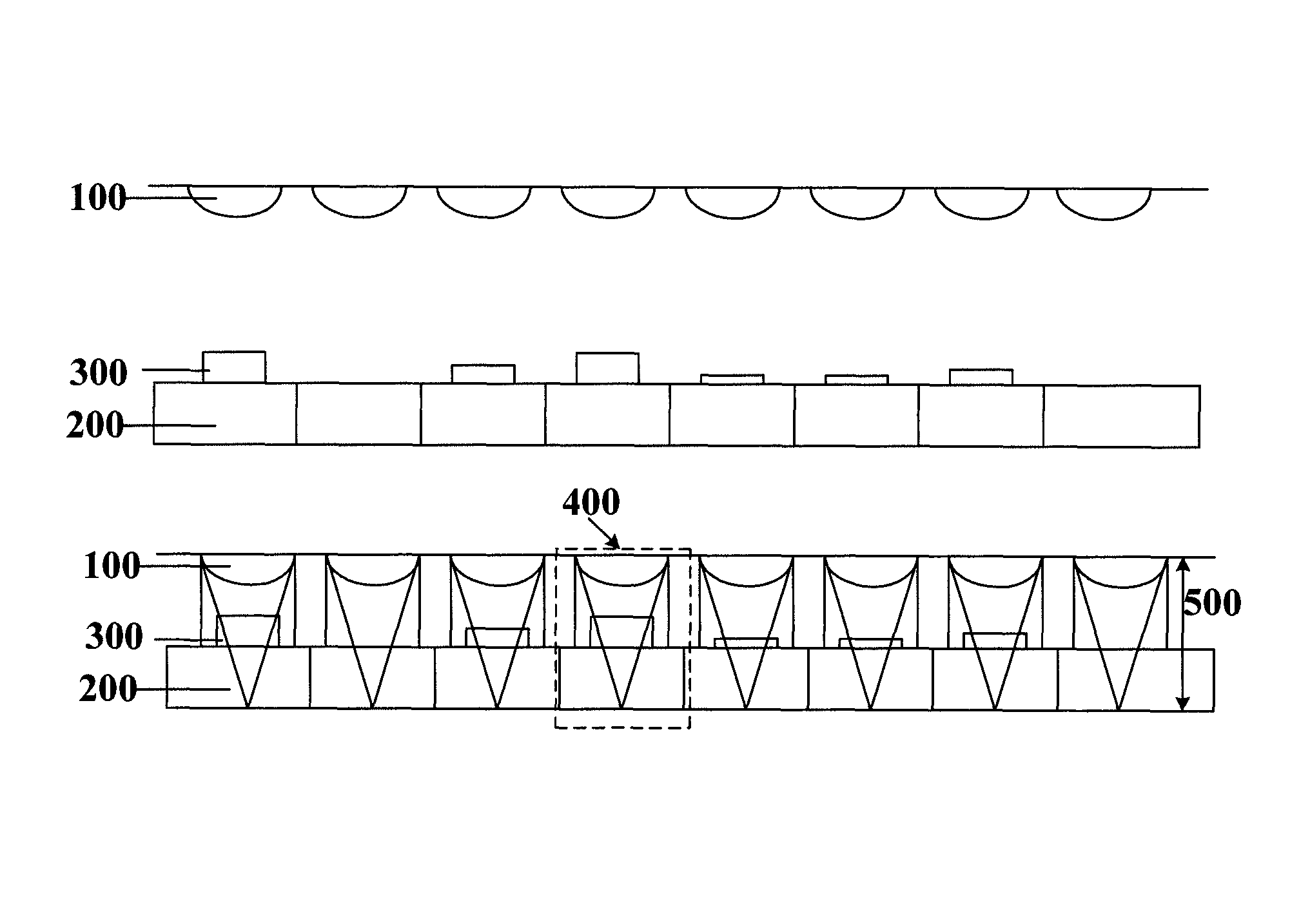
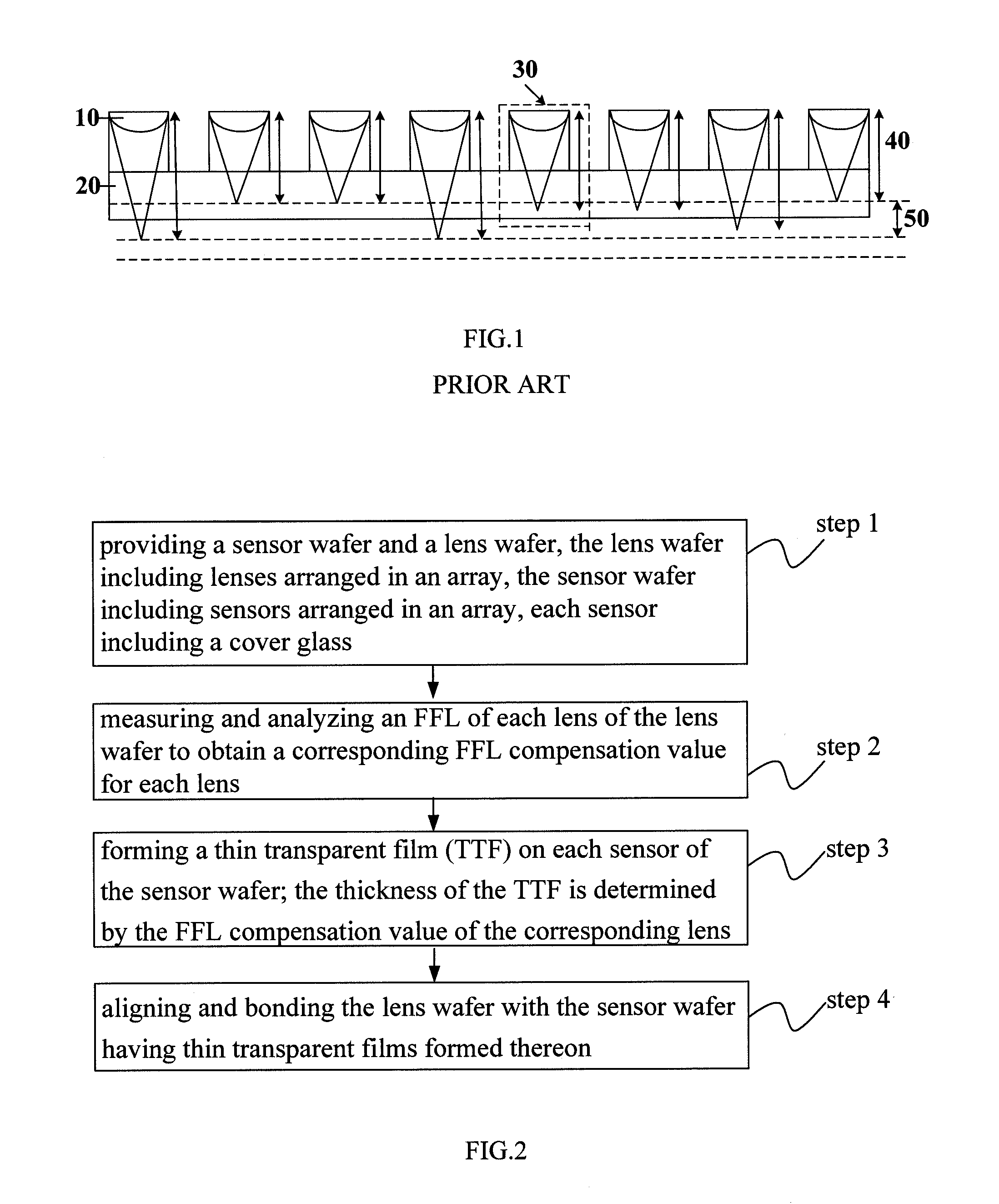
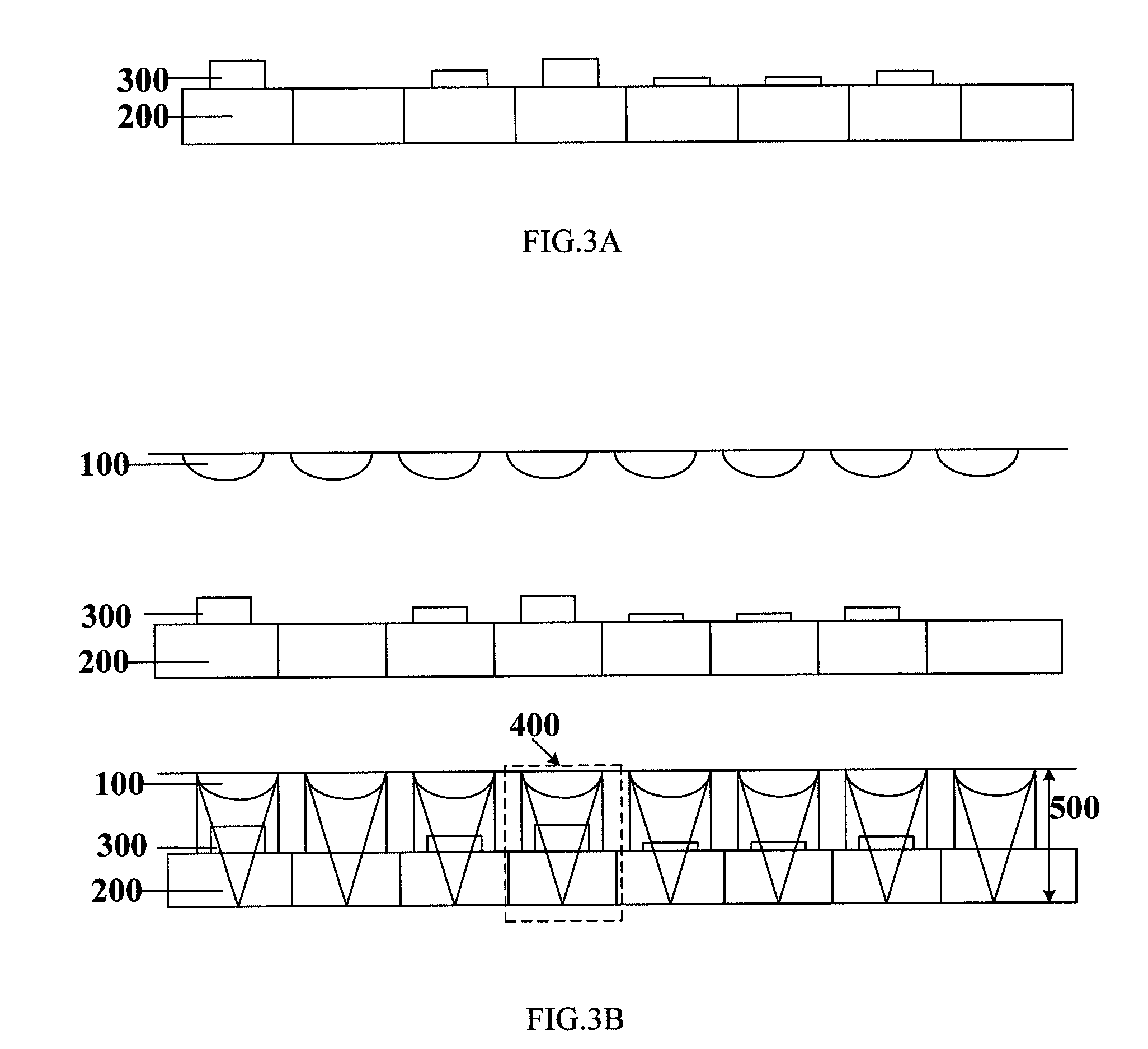
[0029]Detailed analysis on the wafer-level bonding method for fabricating wafer level camera lenses of the present invention will be made below by taking the flow chart shown in FIG. 2 as an example while giving reference to FIG. 3A and FIG. 3B. The method includes the following steps:

[0030]Step 1: a lens wafer and a sensor wafer are respectively produced by using existing fabrication processes. The lens wafer includes lenses 100 arranged in an array a...


PUM


Abstract

A wafer-level bonding method for fabricating wafer level camera lenses is disclosed. The method includes: providing a lens wafer including lenses arranged in an array and a sensor wafer including sensors arranged in an array; measuring and analyzing an FFL of each lens to obtain a corresponding FFL compensation value for each lens; forming a thin transparent film (TTF) on each sensor of the sensor wafer, and the thickness of TTF is determined by the FFL compensation value of the corresponding lens; aligning and bonding the lens wafer with the sensor wafer having TTFs formed thereon. Since the focal length of each lens is adjusted to compensate the FFL of the lens by adding a TTF of transparent optical material with an index of refraction that is similar to the index of refraction of the sensor cover glass, the FFL variation of each camera lens can be reduced.

Description

CROSS-REFERENCES TO RELATED APPLICATIONS[0001]This application claims the priority of Chinese patent application number 201210367894.9, filed on Sep. 27, 2012, the entire contents of which are incorporated herein by reference.TECHNICAL FIELD[0002]The present invention relates to the field of semiconductor manufacturing, and more particularly, to a wafer-level bonding process for fabricating wafer level camera lenses, in which process, a flange focal length (FFL) compensation method is employed.BACKGROUND[0003]Camera is a kind of video input device. The role of a lens in a camera is equivalent to that of human eyes, and the brightness and clearness of the images taken by the camera are dependent on the quality of the lens used. One type of lens manufacturing uses full wafers to manufacture lenses in parallel using wafer processing equipment and forms lens wafers. Since a wafer camera is comprised of one or more bonded lens wafers, the result is that the wafer camera is a 2D array of ...

Claims


Application Information

Patent Timeline
Patent Type & Authority Patents(United States)
IPC IPC(8): H01L21/00G02B3/00G02B7/02G02B13/00H01L21/66H01L27/146
CPCH01L22/12H01L27/14618G02B13/0085H01L22/20H01L27/14687H01L27/14632G02B3/0043H01L2924/0002H01L2924/00
Inventor FAN, REGIS
Owner OMNIVISION TECH (SHANGHAI) CO LTD
Why Eureka
Try Eureka