Semiconductor light emitting device having multi-cell array, light emitting module, and illumination apparatus

a light-emitting device and semiconductor technology, applied in the direction of semiconductor devices, basic electric elements, electrical equipment, etc., can solve the problems of high-power leds using high-rated currents that have low light efficiency, accelerate light efficiency degradation, and reduce light efficiency, so as to improve light extraction efficiency, improve light efficiency, and improve current density per unit area

Active Publication Date: 2014-09-09
SAMSUNG ELECTRONICS CO LTD
View PDF27 Cites 15 Cited by
  • Summary
  • Abstract
  • Description
  • Claims
  • Application Information

AI Technical Summary

Benefits of technology

[0009]An aspect of the present invention provides a semiconductor light emitting device that improves a current density per unit area to improve the light efficiency and also the light extraction efficiency thereof.
[0010]Another aspect of the present invention provides a semiconductor light emitting device that improves a current density per unit area to improve the light efficiency and also uses a reflection structure to improve a light path.
[0011]Another aspect of the present invention provides a semiconductor light emitting device that improves a current density per unit area to improve the light efficiency and also improves the structure and location of a pad to implement a uniform current distribution over all cells.

Problems solved by technology

However, a high-power LED using a high-rated current may have low light efficiency due to a high current density, when compared to a low-power LED using a low-rated current.
Specifically, if a rated current is increased to obtain high luminous flux in an LED chip of the same area in order to obtain high power, the light efficiency may be degraded due to an increase in the current density.
Also, the light efficiency degradation is accelerated due to heat generated by the device.

Method used


Image

  • Semiconductor light emitting device having multi-cell array, light emitting module, and illumination apparatus
  • Semiconductor light emitting device having multi-cell array, light emitting module, and illumination apparatus
  • Semiconductor light emitting device having multi-cell array, light emitting module, and illumination apparatus

Examples


first embodiment

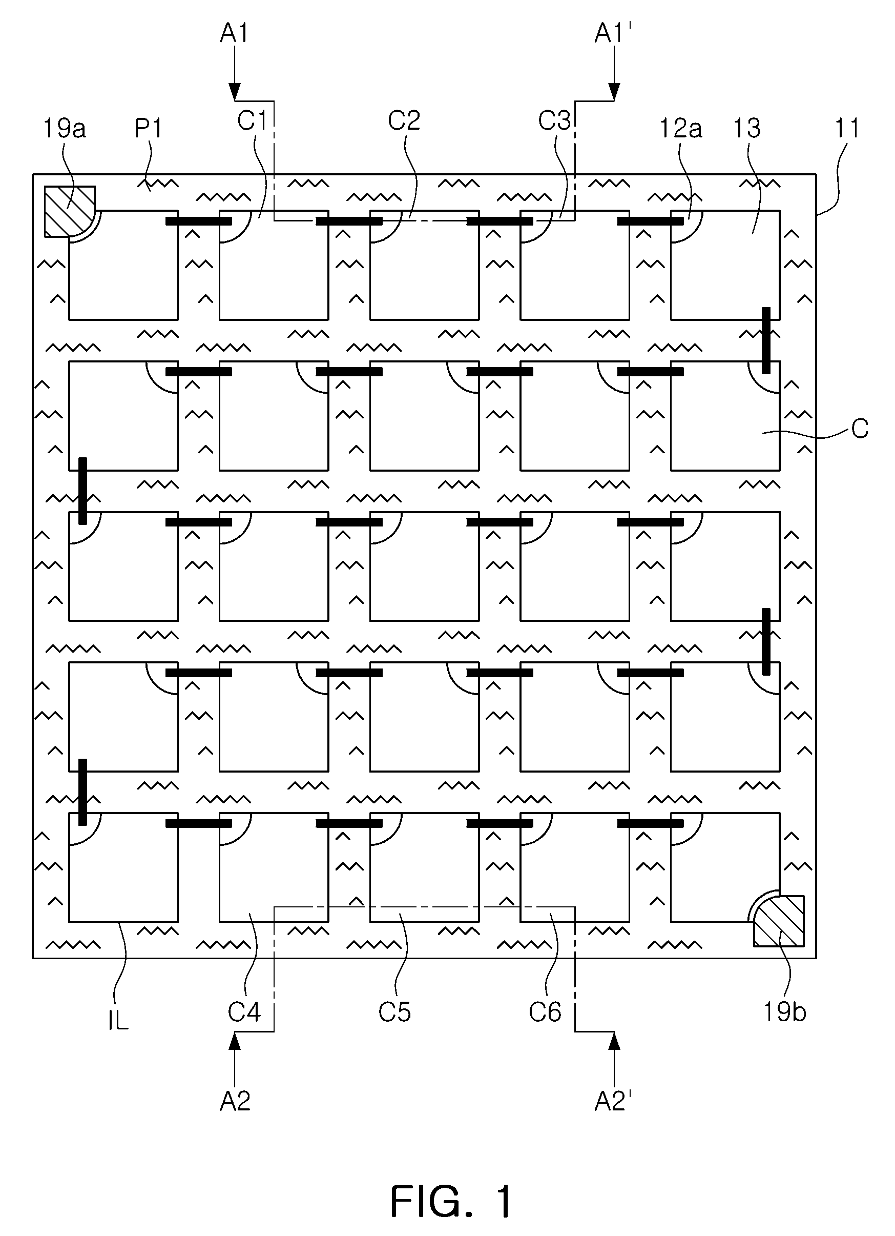
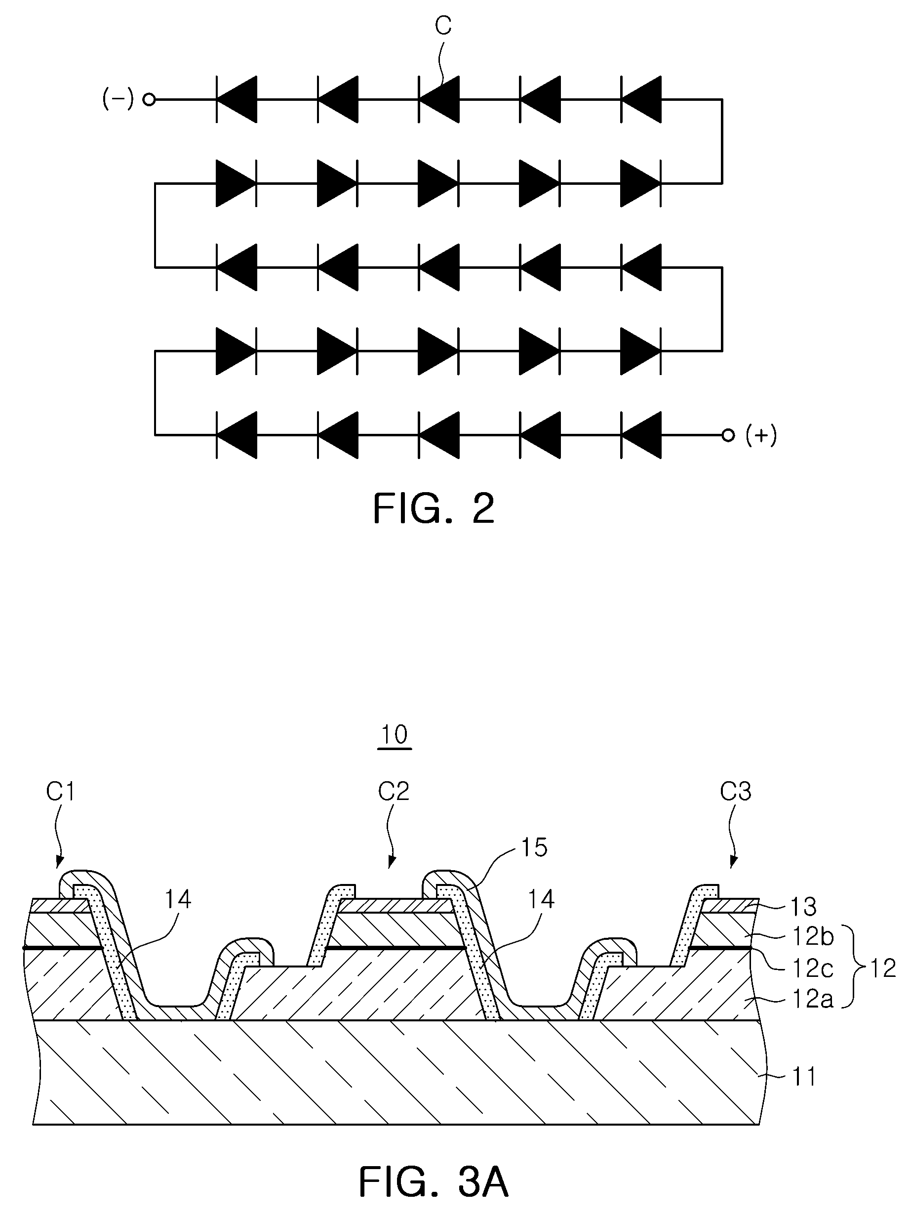
[0056]FIG. 1 is a plan view illustrating an example (a complete isolation between cells) of a multi-cell array semiconductor light emitting device according to the present invention. FIG. 2 is an equivalent circuit diagram illustrating the connection between cells of the multi-cell array semiconductor light emitting device illustrated in FIG. 1. FIGS. 3A and 3B are side sectional views of the multi-cell array semiconductor light emitting device illustrated in FIG. 1, which are taken along lines A1-A1′ and A2-A2′ of FIG. 1.

[0057]Referring to FIGS. 1 and 3A, a multi-cell array semiconductor light emitting device 10 according to a first embodiment of the present invention includes a substrate 11, and a plurality of light emitting cells C arrayed on the top surface of the substrate 11.

[0058]The light emitting cell C is obtained by dividing, through an isolation process, a semiconductor multilayer structure 12 having a first-conductivity-type semiconductor layer 12a, an active layer 12c,...

second embodiment

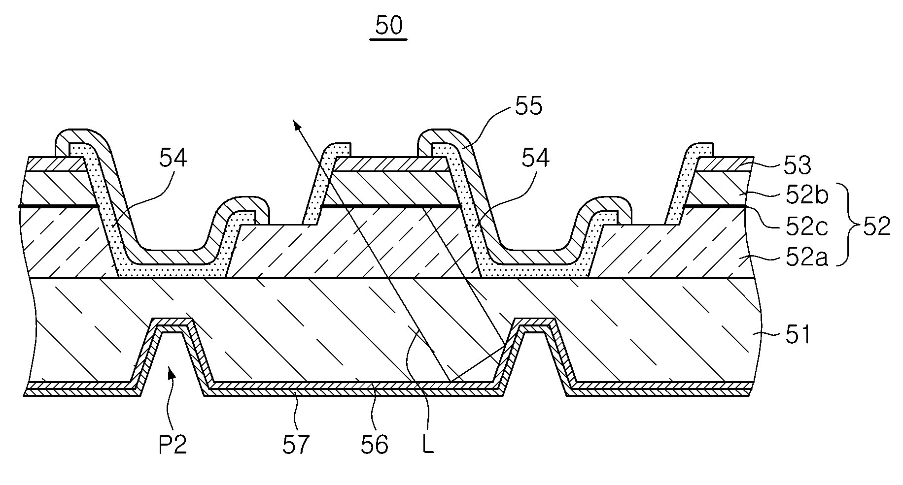
[0104]FIGS. 8A and 8B are cross-sectional views illustrating various examples (a complete isolation between cells) of a multi-cell array semiconductor light emitting device according to the present invention.

[0105]Unlike the embodiment illustrated in FIGS. 3A and 3B, this embodiment provides a scheme for applying a reflection member to the isolation region.

[0106]The structure illustrated in FIG. 8A corresponds to the region of A2-A2′ in the multi-cell array semiconductor light emitting device having a similar array to FIG. 1.

[0107]Referring to FIG. 8A, a semiconductor light emitting device 80 includes a substrate 81, and a light emitting cell having a semiconductor multilayer structure 82 formed on the substrate 81.

[0108]The semiconductor multilayer structure 82 has a first-conductivity-type semiconductor layer 82a, an active layer 82c, and a second-conductivity-type semiconductor layer 82b that are sequentially stacked on the substrate 81.

[0109]As illustrated in FIG. 8A, a reflecti...

third embodiment

[0138]FIG. 12 is a plan view illustrating an example of a multi-cell array semiconductor light emitting device according to the present invention. FIG. 13 is an equivalent circuit diagram of the multi-cell array semiconductor light emitting device illustrated in FIG. 12.

[0139]Referring to FIG. 12, a multi-cell array semiconductor light emitting device 120 includes a substrate 121, and a plurality of light emitting cells C arrayed in a 6×6 pattern on the top surface of the substrate 121.

[0140]The light emitting cell C is obtained by dividing a semiconductor multilayer structure 122 having a first-conductivity-type semiconductor layer 122a, an active layer 122c, and a second-conductivity-type semiconductor layer 122b that are sequentially formed on the top surface of the substrate 121.

[0141]In this embodiment, the isolation process is performed through a complete isolation process that completely removes the semiconductor multilayer structure 122 to expose the surface of the substrate...


PUM


Abstract

A semiconductor light emitting device includes a substrate, a plurality of light emitting cells, a connection part, and a concavo-convex part. The light emitting cells are arrayed on the top surface of the substrate. Each of the light emitting cells has a first-conductivity-type semiconductor layer, an active layer, and a second-conductivity-type semiconductor layer that are sequentially stacked on the top surface of the substrate. The connection part is formed to connect the light emitting cells in series, parallel or series-parallel. The concavo-convex part is formed in at least one of the bottom surface of the substrate and the top surface of an isolation region between the light emitting cells.

Description

CROSS-REFERENCE TO RELATED APPLICATIONS[0001]This application claims the priority of Korean Patent Application No. 10-2010-0015422 filed on Feb. 19, 2010, in the Korean Intellectual Property Office, the disclosure of which is incorporated herein by reference.BACKGROUND OF THE INVENTION[0002]1. Field of the Invention[0003]The present invention relates to a semiconductor light emitting device, and more particularly, to a semiconductor light emitting device having an array of light emitting cells, a light emitting module including the semiconductor light emitting device, and an illumination apparatus including the light emitting module.[0004]2. Description of the Related Art[0005]In general, semiconductor light emitting diodes (LEDs) are advantageous for light sources in terms of power, efficiency and reliability. Therefore, semiconductor LEDs are being actively developed as high-power, high-efficiency light sources for various illumination apparatuses as well as for backlight units of...

Claims


Application Information

Patent Timeline
Patent Type & Authority Patents(United States)
IPC IPC(8): H01L29/18H01L27/15H01L33/20H01L33/46H01L33/60H01L33/62
CPCH01L27/156H01L33/62H01L33/46H01L33/60H01L2224/48091H01L2933/0091H01L33/20H01L2924/00014
Inventor KIM, SUNG TAEKIM, TAE HUNKIM, JAE YOONHA, HAE SOO
Owner SAMSUNG ELECTRONICS CO LTD
Why Eureka
Try Eureka