Display apparatus
a technology of display apparatus and display screen, which is applied in the direction of discharge tube luminescnet screen, discharge tube/lamp details, electric discharge lamps, etc., can solve the problems of unnatural luminance characteristic and increased luminance at the larger radiation angle, and achieve good luminance characteristic
- Summary
- Abstract
- Description
- Claims
- Application Information
AI Technical Summary
Benefits of technology
Problems solved by technology
Method used
Image


Examples
first embodiment
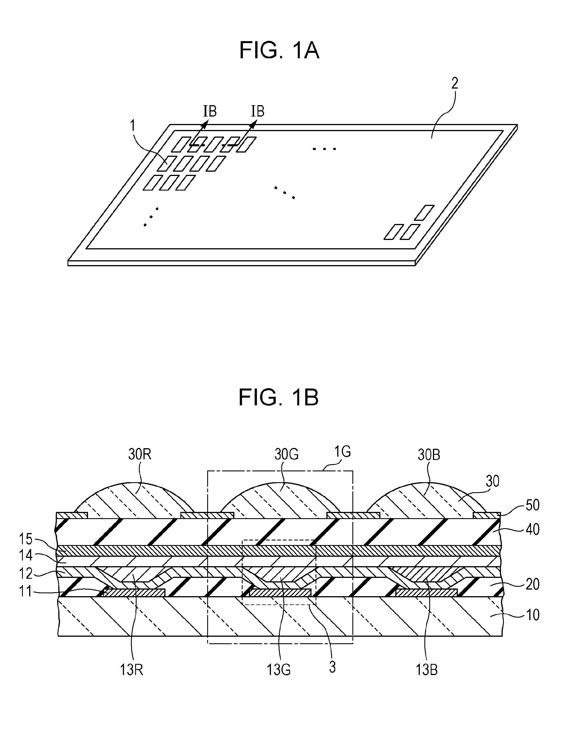
[0023]FIG. 1A is a schematic perspective view of a display apparatus according to a first embodiment of the present invention. The display apparatus according to the first embodiment of the present invention includes a plurality of pixels 1 each including an organic EL element. The plural pixels 1 are arrayed in a matrix pattern, and they form a display region 2. The term “pixel” used herein implies a region corresponding to a luminescent region of one light-emitting element. In the display apparatus according to the first embodiment, the light-emitting element is an organic EL element, and the organic EL element of one color is disposed in one-to-one relation to the pixel 1. A luminescent color of the organic EL element is, e.g., red, green or blue. The luminescent color may be yellow or cyan. Further, the display apparatus according to the first embodiment includes an array of plural pixel units each including a plurality of pixels having different luminescent colors (e.g., a red ...
second embodiment
[0084]FIG. 9A is a schematic sectional view of a display apparatus according to a second embodiment of the present invention. The second embodiment differs from the first embodiment in that an underlying layer 60 is disposed between the light absorbing layer 50 and the lens portion 30 to cover the light absorbing layer 50.
[0085]The underlying layer 60 serves to adjust the respective distances between the lenses 30R, 30G, 30B and the luminescent layers 13R, 13G, 13B. Further, the underlying layer 60 may have the function of planarizing the surface of the light absorbing layer 50.
[0086]The underlying layer 60 can be formed by using, e.g., a negative resist (OMR-83 made by TOKYO OHKA KOGYO Co., Ltd. or SU-8 made by NIPPON KAYAKU Co., Ltd.), a photo-curable resin (KZ6666 made by JSR), or a thermosetting resin absorbing an ultraviolet ray (HALS hybrid UV-G made by NIPPON SHOKUBai CO., LTD.). The optical transmittance of the underlying layer 60 is to be 80% or more in the visible light ra...
third embodiment
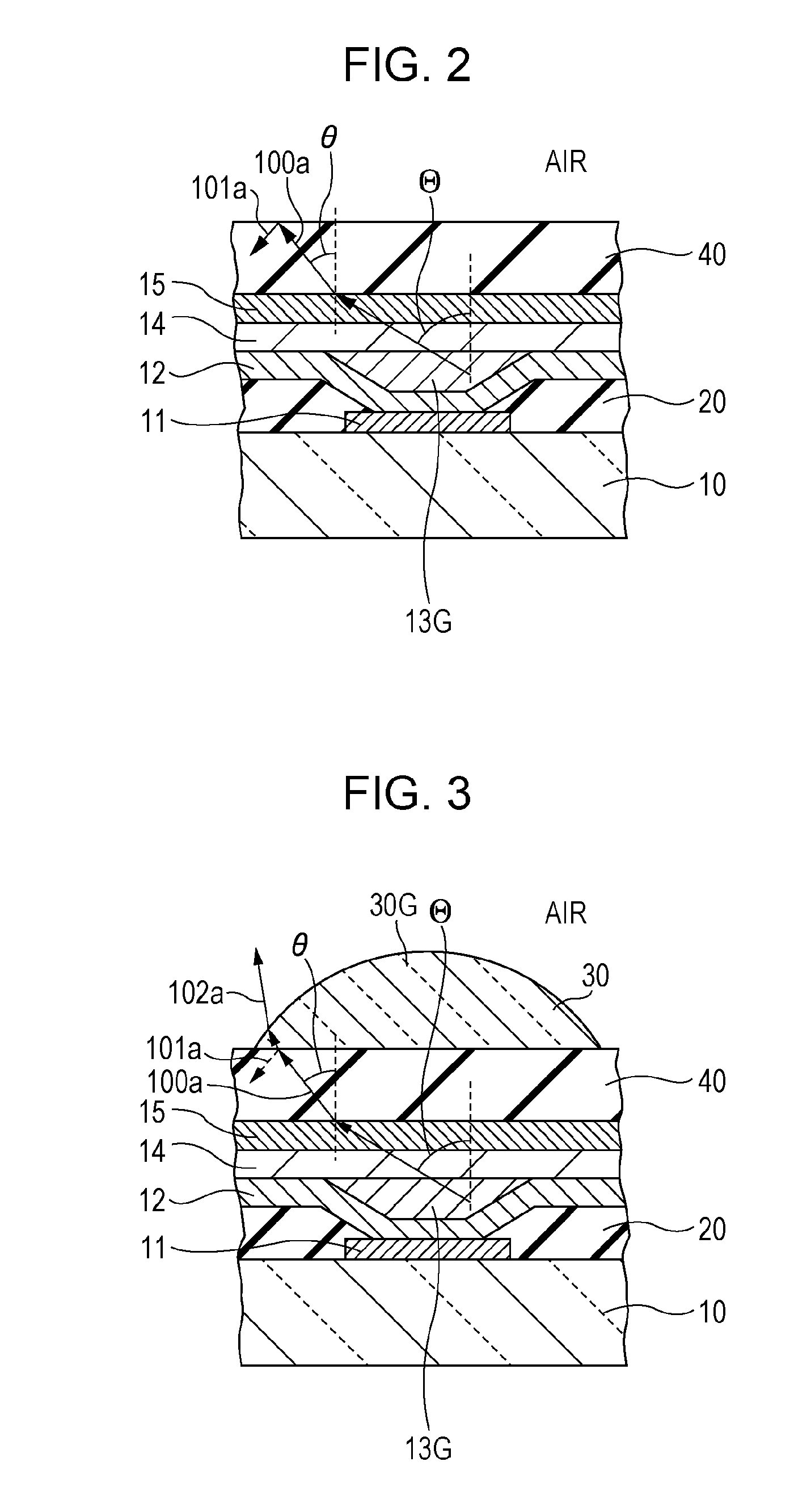
[0087]FIG. 9B is a schematic sectional view of a display apparatus according to a third embodiment of the present invention. The third embodiment differs from the first embodiment in that the light absorbing layer 50 is disposed on the lens portion 30.
[0088]In the first embodiment, the light absorbing layer 50 is disposed closer to the organic EL element than the lens such that the light radiated at a larger angle than θB, at which the light intensity distribution of the light radiated from the organic EL element 3 into the protective layer 40 with respect to the radiation angle takes the local minimum value, does not enter the lens. On the other hand, in the third embodiment, the light absorbing layer 50 is disposed on the side closer to the outside than the lens in the light radiation direction (i.e., on the emergent side rather than the incident side of the lens) such that the light radiated at a larger angle than θB is not output to the outside of the display apparatus through t...
PUM
 Abstract
Description
Claims
Application Information