

Preparation method for copper oxide nanowires
a technology of copper oxide and nanowires, which is applied in the field of preparation of copper oxide nanowires, can solve the problems of difficult control of uniformity of deposited film and high cost of equipment use, and achieve the effect of reducing manufacturing cost and reducing the technology flow of coating
- Summary
- Abstract
- Description
- Claims
- Application Information
AI Technical Summary
Benefits of technology
Problems solved by technology
Method used
Image

Examples
example 1
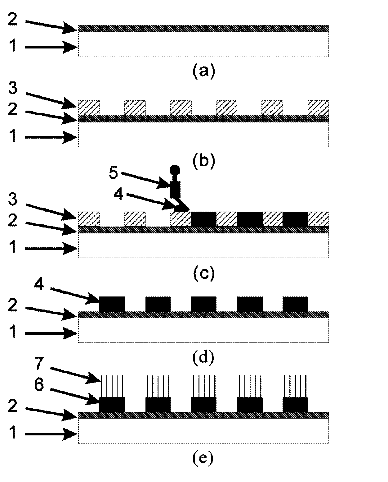
[0037]A process of preparing copper oxide nanowires on a substrate which is a ITO glass is illustrated.
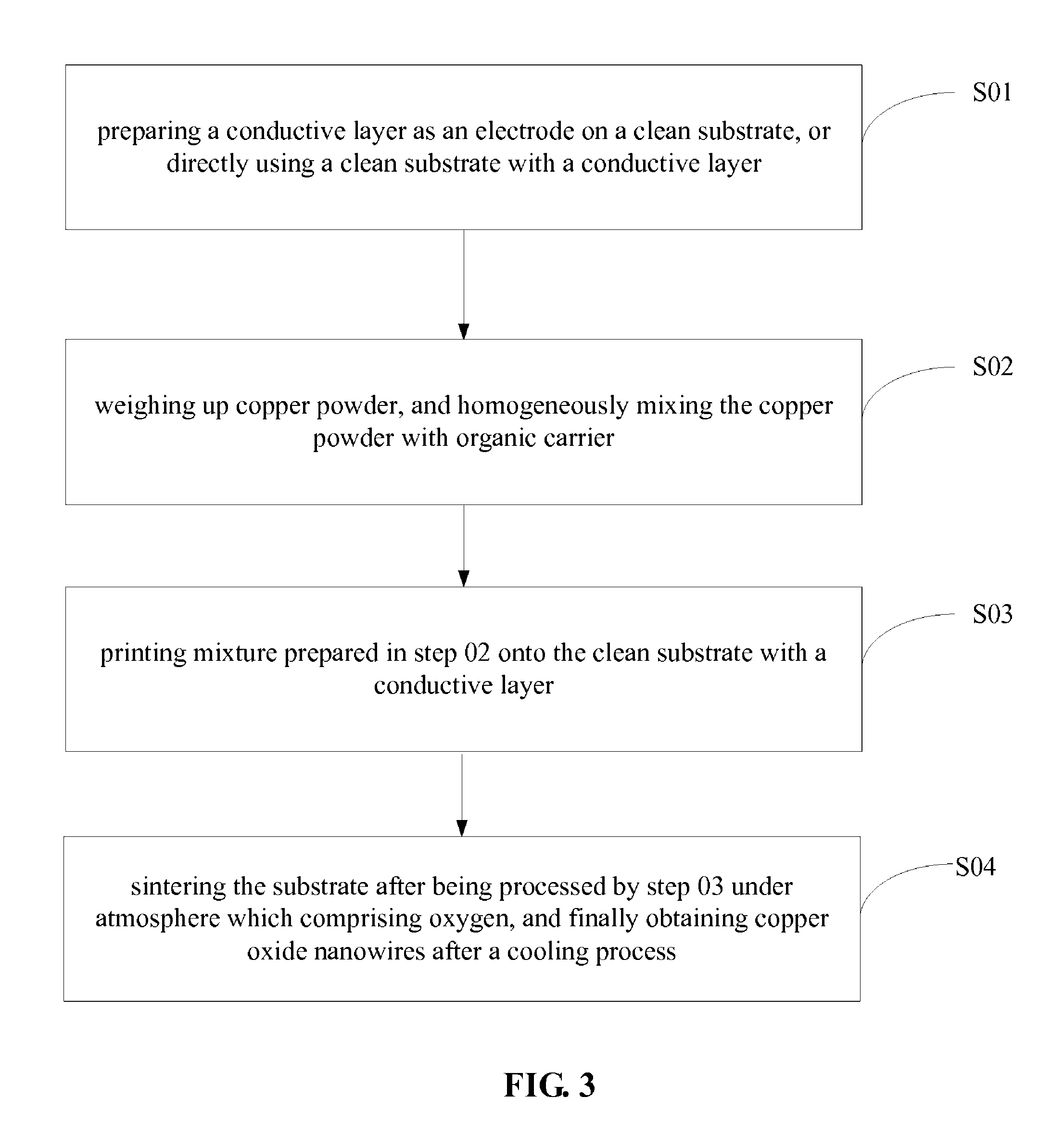
[0038]Size of the glass is 40 mm×50 mm×3 mm. Graphics printed on the ITO glass is a square having a size of 25 mm×25 mm. Firstly, 7 g of organic carrier weighted up is poured in to a flask having a capacity of 10 ml, then 21 g of copper powder with purity is 99.9%, and having a diameter of 20 μm. Secondly, the organic carrier is stirred by a mixer, and at the same time the copper powder is gradually added to the organic carrier, keep stirring for 24 hours. Thirdly, the ITO glass is put into acetone, ethanol, and deionized water in turn to ultrasonic clean for 15 minutes, then dried or blow-dried with inert gas. The preparation process shown in FIG. 1 is employed, mixture containing copper powder is screen printed on the ITO glass to form a layer having a thick of 40 μm. Copper powder matrix printed on the ITO glass is put into a heating furnace, temperature is increased to 450° C. ...
example 2
[0039]A process of preparing copper oxide nanowires on a substrate which is common glass is illustrated.
[0040]Size of the glass is 60 mm×60 mm×1.1 mm. Graphics printed on the glass is circular having a diameter of 30 mm. Firstly, 8 g of organic carrier weighted up is poured in to a flask having a capacity of 10 ml, then 28 g of copper powder with purity is 99.9%, and having a diameter of 20 μm. Secondly, the organic carrier is stirred by a mixer, and at the same time the copper powder is gradually added to the organic carrier, keep stirring for 24 hours. Thirdly, the glass is put into acetone, ethanol, and deionized water in turn to ultrasonic clean for 15 minutes, then dried or blow-dried with inert gas. The preparation process shown in FIG. 1 is employed, a chrome layer having a thickness of 2 μm as a conductive layer is deposited on the glass by a magnetron sputtering equipment. Mixture containing copper powder is screen printed on the chrome layer to form a layer having a thick ...
example 3
[0041]A process of preparing copper oxide nanowires on a substrate which is ceramics sheet is illustrated.
[0042]Size of the ceramics sheet is 50 mm×60 mm×1 mm. Graphics printed on the ceramics sheet is rectangular having a size of 25 mm×40 mm. Firstly, 10 g of organic carrier weighted up is poured in to a flask having a capacity of 10 ml, then 28 g of copper powder with purity is 99.9%, and having a diameter of 300 μm. Secondly, the organic carrier is stirred by a mixer, and at the same time the copper powder is gradually added to the organic carrier, keep stirring for 24 hours. Thirdly, the ceramics sheet is put into acetone, ethanol, and deionized water in turn to ultrasonic clean for 15 minutes, then dried or blow-dried with inert gas. The preparation process shown in FIG. 1 is employed, conductive silver starch is screen printed on the ceramics sheet to form a entirely conductive layer having a thickness of 200 μm. Mixture containing copper powder is screen printed on the conduc...
PUM
| Property | Measurement | Unit |
|---|---|---|
| thickness | aaaaa | aaaaa |
| diameter | aaaaa | aaaaa |
| thickness | aaaaa | aaaaa |
Abstract
Description
Claims
Application Information