Gallium nitride substrate and epitaxial wafer

a technology of gallium nitride and substrate, applied in the direction of basic electric elements, electrical apparatus, semiconductor devices, etc., can solve the problems of abnormal growth of epitaxial growth layer, reduced speed, and difficult to prevent physical level differences, etc., to achieve good crystalline quality and good flatness

Inactive Publication Date: 2014-10-07
SUMITOMO CHEM CO LTD
View PDF9 Cites 1 Cited by
  • Summary
  • Abstract
  • Description
  • Claims
  • Application Information

AI Technical Summary

Benefits of technology

[0021]According to one embodiment of the invention, a gallium nitride substrate can be provided that is capable of growing an epitaxial growth layer having a good crystalline quality even if the surface has physical level differences. Also, an epitaxial wafer can be provided that a surface thereof has good flatness by growing the epitaxial growth layer on the above-mentioned gallium nitride substrate.

Problems solved by technology

However, even if the polishing is carried out such that the grain diameter of loose grain is lessened, polishing speed is reduced and polishing time is prolonged by using the method described in JP-A-2001-322899, it is extremely difficult to prevent physical level differences due to scratch or the like from occurring in the whole surface of the gallium nitride substrate.
If an epitaxial growth layer is grown on a surface having physical level differences, even if the dimension of the physical level differences is several nanometers, it may be caused that the epitaxial growth layer is abnormally grown, so that the surface is not planarized.
In case of manufacturing an optical device by using the above-mentioned epitaxial wafer, a problem is caused that defect due to decrease in emission intensity is raised so that production yield is reduced.

Method used


Image

  • Gallium nitride substrate and epitaxial wafer
  • Gallium nitride substrate and epitaxial wafer
  • Gallium nitride substrate and epitaxial wafer

Examples


embodiments

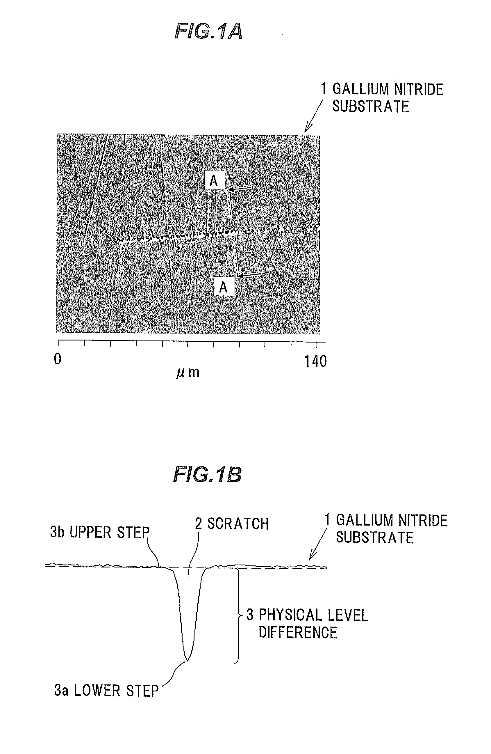
[0027]As the result of earnest investigation of the inventors et al., it has been found that even if physical level differences due to scratches and the like exist in the surface of the gallium nitride substrate, a good epitaxial crystal growth is not always impossible, but if the dimension of the physical level difference is relatively small, and a difference of a cathodoluminescence emission intensity of a wavelength corresponding to a bandgap of the gallium nitride substrate between an upper step and a lower step of the physical level difference is small, it is possible to prevent the crystal on the substrate from abnormally being grown so as to allow the crystal having a flat surface to be grown.

[0028]The cathodoluminescence emission intensity is varied dependent on the crystal condition in the measurement place, thus a large difference of the cathodoluminescence emission intensity between the upper step and the lower step of the physical level difference represents that the cry...

example 1

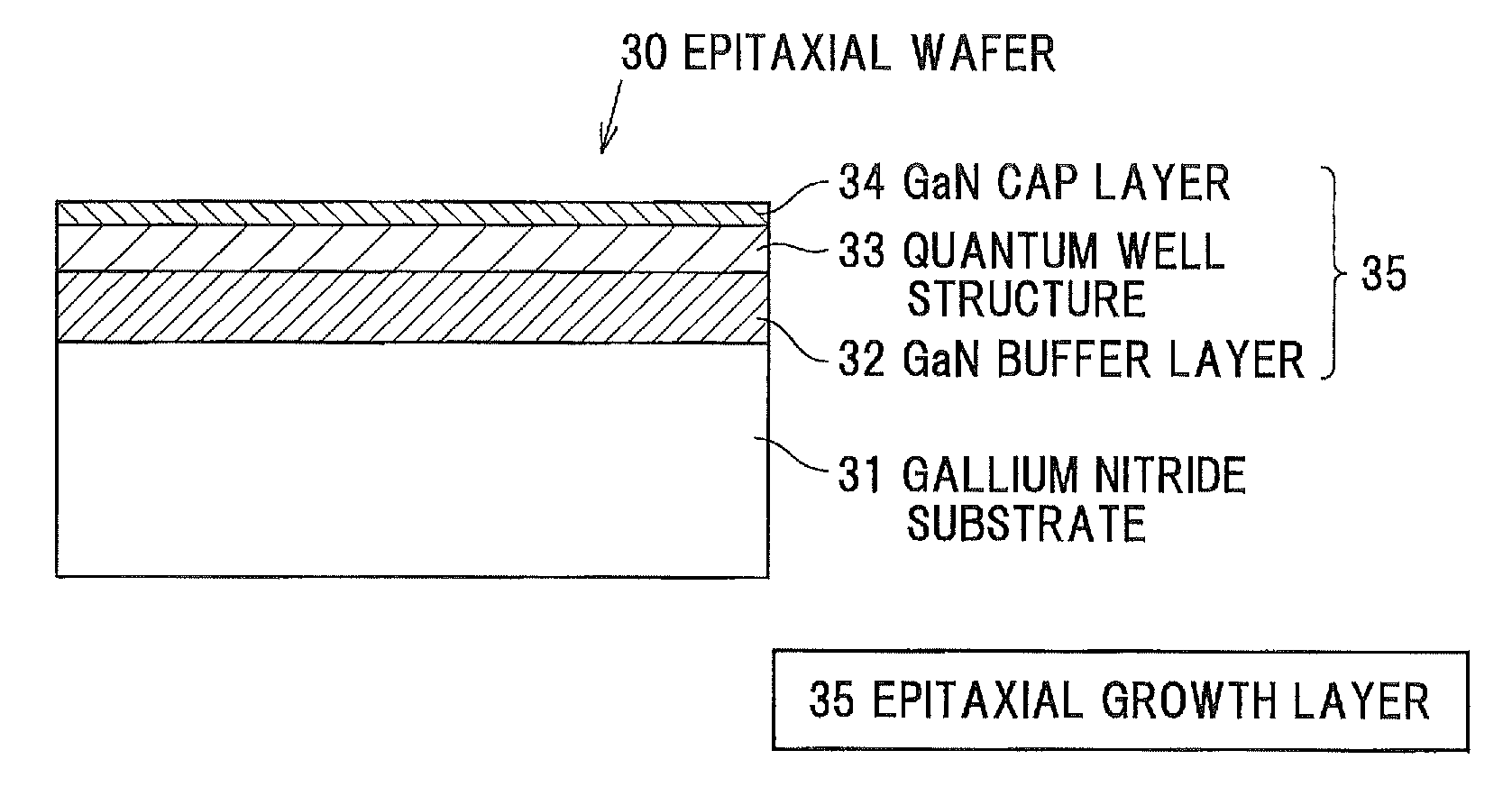
[0052]In Example 1, 25 gallium nitride substrates were formed by VAS method. Next, with regard to each substrate, the physical level difference was measured by using a three-dimensional optical profiler, and 20 evaluation regions were determined with respect to each dimension of the physical level difference. Next, the cathodoluminescence measurement was carried out in each evaluation region of each substrate. Next, an epitaxial growth layer was grown on each gallium nitride substrate so as to form a quantum well structure, thereby an epitaxial wafer was obtained. Next, the photoluminescence measurement was carried out with respect to each epitaxial wafer, an average measurement value in each evaluation region was obtained, and the flatness of the surface was evaluated, so as to investigate a relationship with the dimension of the physical level difference and the result of cathodoluminescence measurement. Hereinafter, a concrete process will be explained.

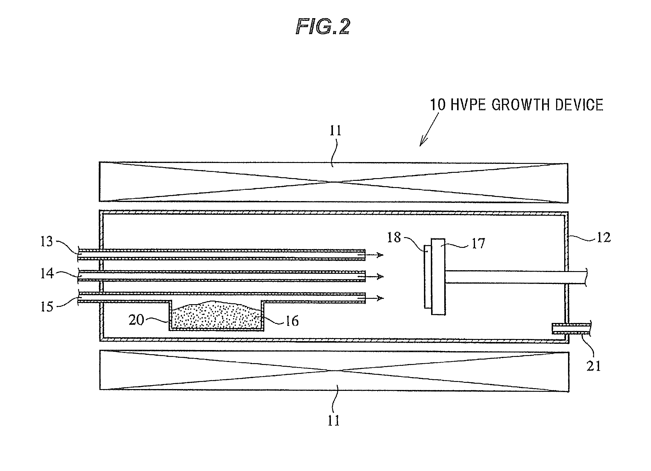
[0053]Manufacture of Galliu...


PUM


Abstract

A gallium nitride substrate includes a plurality of physical level differences in a surface thereof. All the physical level differences existing in the surface have a dimension of not more than 4 μm. A relationship of (H−L) / H×100≦80 is satisfied in all the physical level differences, where H represents a higher value of cathodoluminescence emission intensities of a wavelength corresponding to a bandgap of the gallium nitride substrate, and L represents a lower value of the cathodoluminescence emission intensities, the cathodoluminescence emission intensities being measured in an upper step and a lower step of the physical level difference.

Description

[0001]The present application is based on Japanese patent application No. 2012-069353 filed on Mar. 26, 2012, the entire contents of which are incorporated herein by reference.BACKGROUND OF THE INVENTION[0002]1. Field of the Invention[0003]This invention relates to a gallium nitride substrate and an epitaxial wafer using the gallium nitride substrate.[0004]2. Description of the Related Art[0005]As a method of manufacturing a good and large gallium nitride substrate, methods are known, such as a method configured to obtain a nitride substrate by Disclosure Elimination by the Epi-growth with Inverted-Pyramidal Pits (DEEP) method (for example, refer to JP-B-3864870) or Void-Assisted Separation (VAS) method (for example refer to JP-A-2004-269313), and a method configured to obtain a GaN freestanding substrate by thickly growing a single crystal of gallium nitride on a heterogeneous substrate by Hydride Vapor Phase Epitaxy (HVPE) method, and separating it from the heterogeneous substrate...

Claims


Application Information

Patent Timeline
Patent Type & Authority Patents(United States)
IPC IPC(8): H01L29/06H01L21/02H01L29/20
CPCH01L29/2003H01L21/0262H01L21/02505H01L21/02458H01L21/02389H01L21/0254Y10S438/962
Inventor YAMAMOTO, SHUNSUKE
Owner SUMITOMO CHEM CO LTD
Why Eureka
Try Eureka