Semiconductor process

a technology of semiconductor components and process steps, applied in the direction of semiconductor/solid-state device manufacturing, basic electric elements, electric apparatus, etc., can solve the problems of serious degradation of semiconductor components, and achieve the effect of improving device performance and reducing the decay rate of nitrogen concentration upon time decreas

Active Publication Date: 2014-11-18
UNITED MICROELECTRONICS CORP
View PDF10 Cites 2 Cited by
  • Summary
  • Abstract
  • Description
  • Claims
  • Application Information

AI Technical Summary

Benefits of technology

[0009]According to the above description, the present invention provides a semiconductor process, which forms a nitrogen containing liner by performing a decoupled plasma nitridation process, and then performs a nitrogen containing annealing process on the nitrogen containing liner. By doing this, the nitrogen containing liner can reduce the inverse narrow width effect (INWE) and therefore improve the device performances. Due to the nitrogen containing annealing process being performed on the nitrogen containing liner after the decoupled plasma nitridation process is performed, the nitrogen concentration in the nitrogen containing liner increases and the reduction of the nitrogen concentration decay upon time decreases.

Problems solved by technology

However, as size scales down, the inverse narrow width effect (INWE) becomes more important, leading performances of the semiconductor components to degrade seriously, wherein the inverse narrow width effect (INWE) is the effect of the threshold voltage of a transistor reducing as the channel width of the transistor reduces.

Method used


Image

  • Semiconductor process
  • Semiconductor process
  • Semiconductor process

Examples


Embodiment Construction

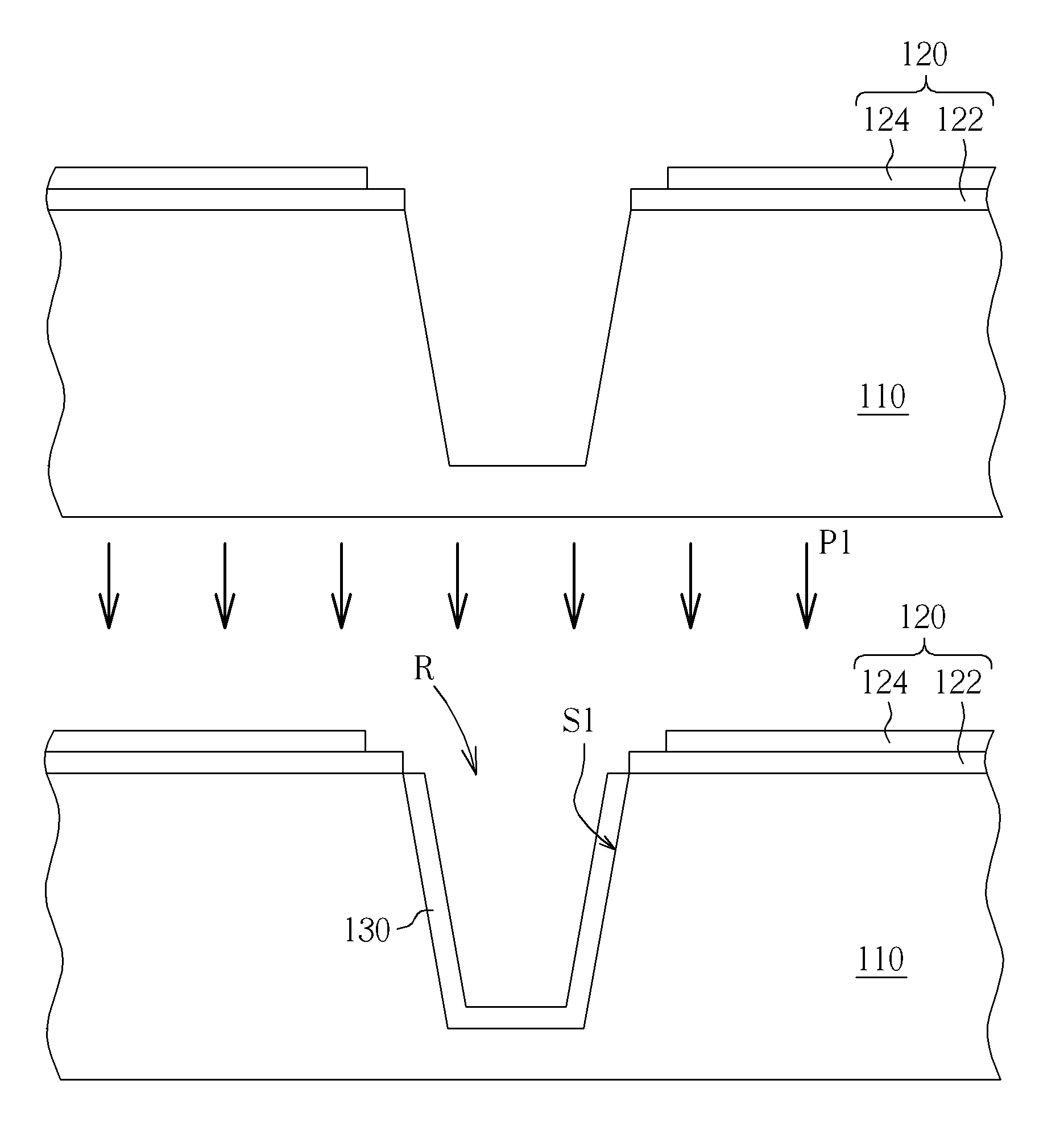
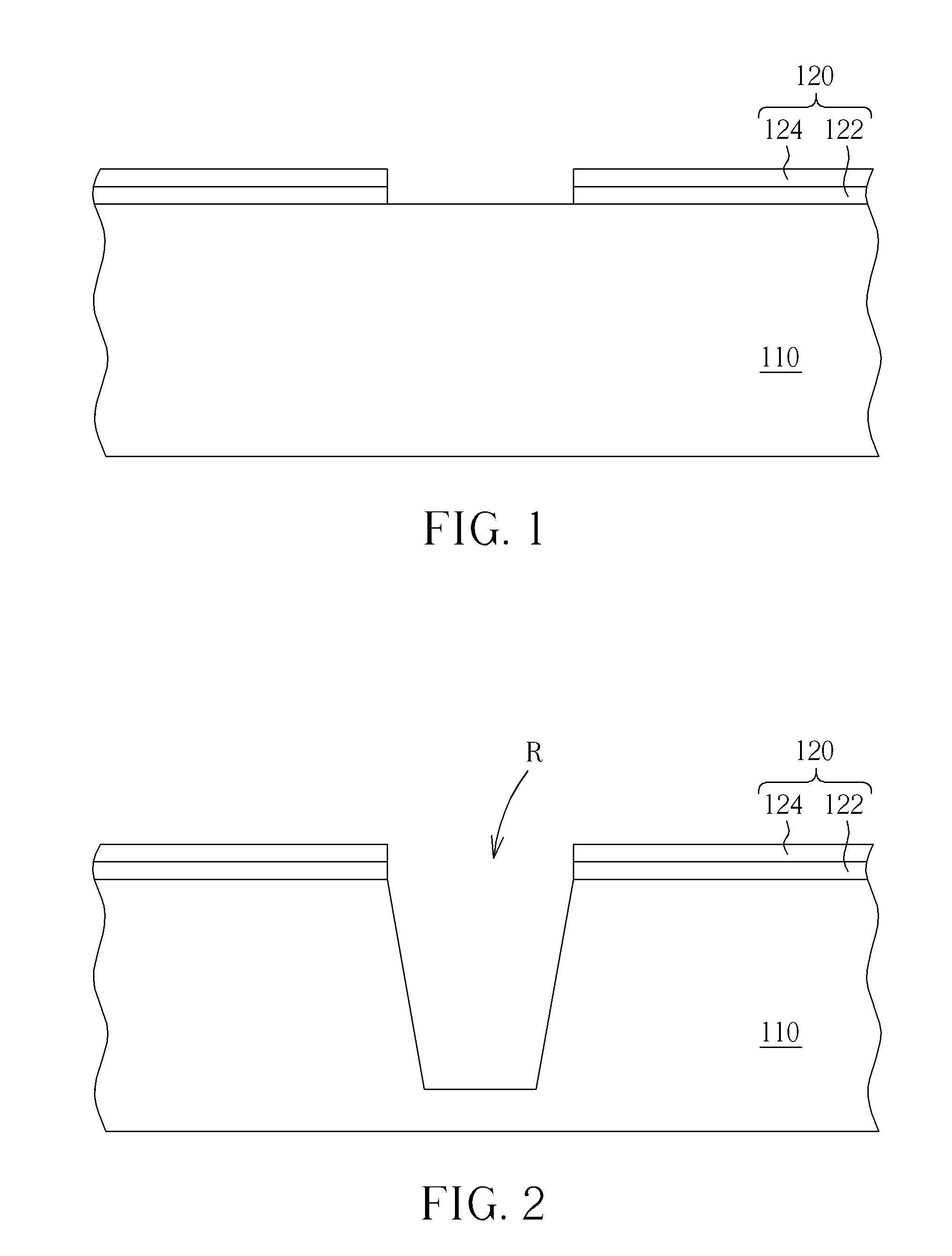
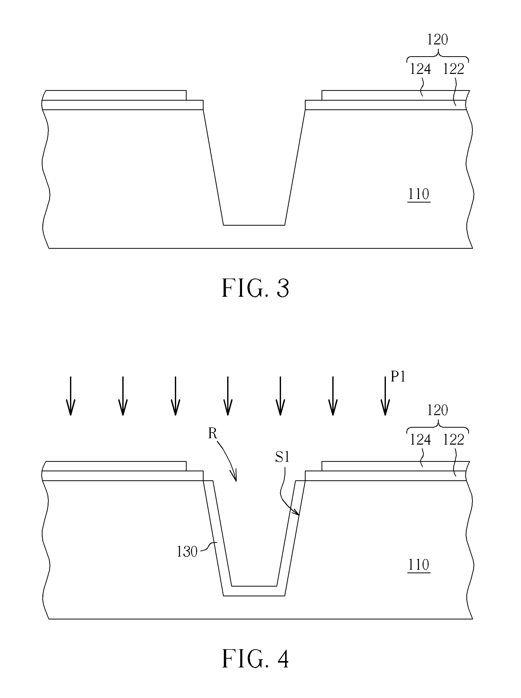
[0014]FIGS. 1-7 schematically depict a cross-sectional view of a semiconductor process according to the first embodiment of the present invention. As shown in FIGS. 1-2, a substrate 110 having a recess R is provided. As shown in FIG. 1, the substrate 110 is provided, wherein the substrate 110 may be a semiconductor substrate such as a silicon substrate, a silicon containing substrate, a III-V group-on-silicon (such as GaN-on-silicon) substrate, a graphene-on-silicon substrate or a silicon-on-insulator (SOI) substrate. A hard mask layer (not shown) is formed on the substrate 110 and is patterned to form a patterned hard mask layer 120. The steps of forming the patterned hard mask layer 120 may include: forming a patterned photoresist (not shown) on the hard mask layer (not shown) by performing a photolithography process, wherein the pattern of the photoresist (not shown) defines the location of the recess R to form below. The hard mask layer (not shown) is patterned by the pattern of...


PUM

PropertyMeasurementUnit
temperatureaaaaaaaaaa
processing timeaaaaaaaaaa
widthaaaaaaaaaa

Abstract

A semiconductor process includes the following steps. A substrate having a recess is provided. A decoupled plasma nitridation process is performed to nitride the surface of the recess for forming a nitrogen containing liner on the surface of the recess. A nitrogen containing annealing process is then performed on the nitrogen containing liner.

Description

BACKGROUND OF THE INVENTION[0001]1. Field of the Invention[0002]The present invention relates generally to a semiconductor process, and more specifically, to a semiconductor process, which forms a nitrogen containing liner by performing a decoupled plasma nitridation process and a nitrogen containing annealing process.[0003]2. Description of the Prior Art[0004]In semiconductor processes, in order to provide good electrical isolation and to prevent short-circuits between electric devices on a wafer, a localized oxidation isolation (LOCOS) process, or a shallow trench isolation (STI) process is used to insulate and protect devices. Since the field oxide layer of the LOCOS process consumes a large area on the wafer, and since bird's beaks can occur when growing the field oxide, an STI process is typically used in the semiconductor processes when the line width is below 0.25 μm.[0005]An STI process involves first forming a shallow trench between each device, and then filling the trench ...

Claims


Application Information

Patent Timeline
Patent Type & Authority Patents(United States)
IPC IPC(8): H01L21/318H01L21/76H01L21/762H01L21/02
CPCH01L21/76237H01L21/02329H01L21/76224H01L21/3185H01L21/02247
Inventor SUN, TE-LINLIN, CHIEN-LIANGWANG, YU-RENYEN, YING-WEI
Owner UNITED MICROELECTRONICS CORP
Why Eureka
Try Eureka