Liquid crystal device

a liquid crystal and film technology, applied in static indicating devices, instruments, non-linear optics, etc., can solve the problems of requiring mechanical manipulation, i.e. removal of film, and the light control film always absorbs a significant fraction of the incident light, etc., to achieve symmetric viewing angle, wide viewing angle properties, and good public mode

Active Publication Date: 2014-11-25
SHARP KK
View PDF58 Cites 5 Cited by
  • Summary
  • Abstract
  • Description
  • Claims
  • Application Information

AI Technical Summary

Benefits of technology

[0060]It is thus possible to provide a novel pixel geometry and driving method for vertically aligned nematic liquid crystal displays. Such techniques allows, for example, a single liquid crystal layer to display an image in two possible modes, one of which has wide viewing angle properties (public mode) and the other in which the image is only discernible from a restricted range of viewing angles (private mode). In both modes, the image is of substantially the same brightness, resolution and quality (contrast, motion response time etc) as the equivalent conventional LCD containing the same number of independently switching display elements (sub-pixels).
[0061]In the public mode, the display may operate as a standard “Advanced Super View” (ASV) (IDW '02 Digest, pp 203-206) or Multidomain Vertical Alignment (MVA) (SID '98 Digest, p1077) type panel in which the LC director is aligned normal to the surface of the cell substrates and an out-of plane electric field applied between electrodes on opposing cell substrates causes the director to tilt down into the plane of the substrate, thereby determining the transmission of light through that pixel. Within each of at least some sub-pixel regions, the director may tilt into a number of azimuthal directions (multidomains) due to the influence of the applied field, for example, as determined by the electrode geometry and / or by shaped protrusions on the surface of the cell substrates, thereby generating a very symmetric viewing angle property and good public mode.

Problems solved by technology

The principal limitation of such films is that they require mechanical manipulation, i.e. removal of the film, to change the display between the public and private viewing modes.
This method has the disadvantages that it contains moving parts which may fail or be damaged and that it adds bulk to the display.
They share the disadvantage that the light control film always absorbs a significant fraction of the light incident upon it, whether the display is in public or private mode.
The display is therefore inefficient in its use of light.
Another disadvantage relates to the power consumption of these devices.
This is a disadvantage for displays which are used for most of the time in the public mode.
The first disadvantage of this method is in the difficulty and expense of manufacturing liquid crystal cells with an appropriate shape.
A second disadvantage is that, in the private mode, a ray of light may enter at an angle such that it passes first through the transparent material and then through part of a liquid crystal cell.
Such a ray will not be completely absorbed by the liquid crystal cell and this may reduce the privacy of the device.
First, due to unwanted diffraction of light from the display by the hologram, the colour of the image seen by viewers is incorrect.
Second, for applications using a touch screen mounted on the front of the display, the user's hand can block the illumination of the hologram and so reduce the effectiveness of the privacy.
However, when the display is viewed from a different angle, different pixels are viewed through the retarder elements and the image is corrupted.
The above methods all suffer the disadvantage that they require the addition of extra apparatus to the display to provide the functionality of electrically switching the viewing angle range.
This adds cost and particularly bulk to the display, which is very undesirable, particularly in mobile display applications such as mobile phones and laptop computers.
However, the viewing angle of a single tilt domain of the VAN mode described is not sufficiently narrow to provide good privacy.
These methods have the disadvantage that not all the sub-pixel regions of the panel are used to display image data to the on-axis viewer, so the display loses both brightness and resolution compared to a standard LCD containing the same number of independent TFT switched sub-pixels, in which all are displaying information to the on-axis viewer.
In the narrow viewing angle mode, one region is driven with a different voltage to the other, resulting in an overall asymmetry for the display and an image which is obscured to the side viewer.
However, this method also results in reduced display resolution and reduced brightness in the private mode.
However, all of these methods necessarily reduce the quality of the displayed image to the legitimate viewer in the private mode.
This method maintains nearly full brightness and resolution of the display in both modes, but it is only applicable to IPS type displays and it is believed that the privacy performance is not as strong as that from the type of display described here.
This scheme also, while maintaining the original display brightness and resolution, provides insufficient privacy strength.
This scheme however adds greatly to the complexity of the display panel and results in greatly reduced transmissive aperture in the display, thus reducing brightness.
However, the method outlined in the document, which uses only single layer electrodes on both substrates, has been shown to be problematic due to the gaps between the electrodes which provide the in-plane field disrupting the LC alignment in the public mode and degrading the wide viewing angle.
This effect has been shown to have a privacy performance which is not as strong as that of the device described here, however.

Method used


Image

  • Liquid crystal device
  • Liquid crystal device
  • Liquid crystal device

Examples


Embodiment Construction

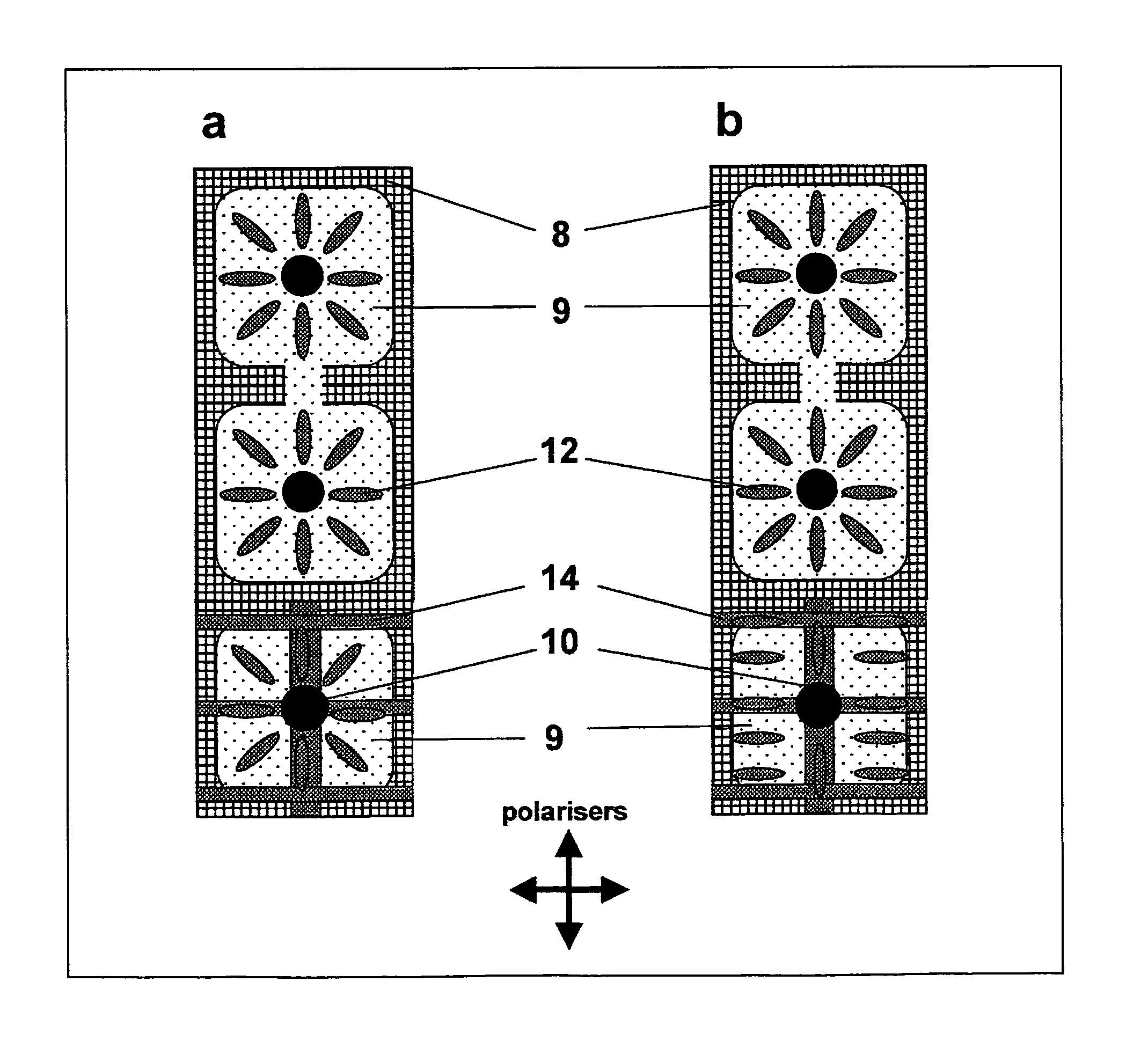
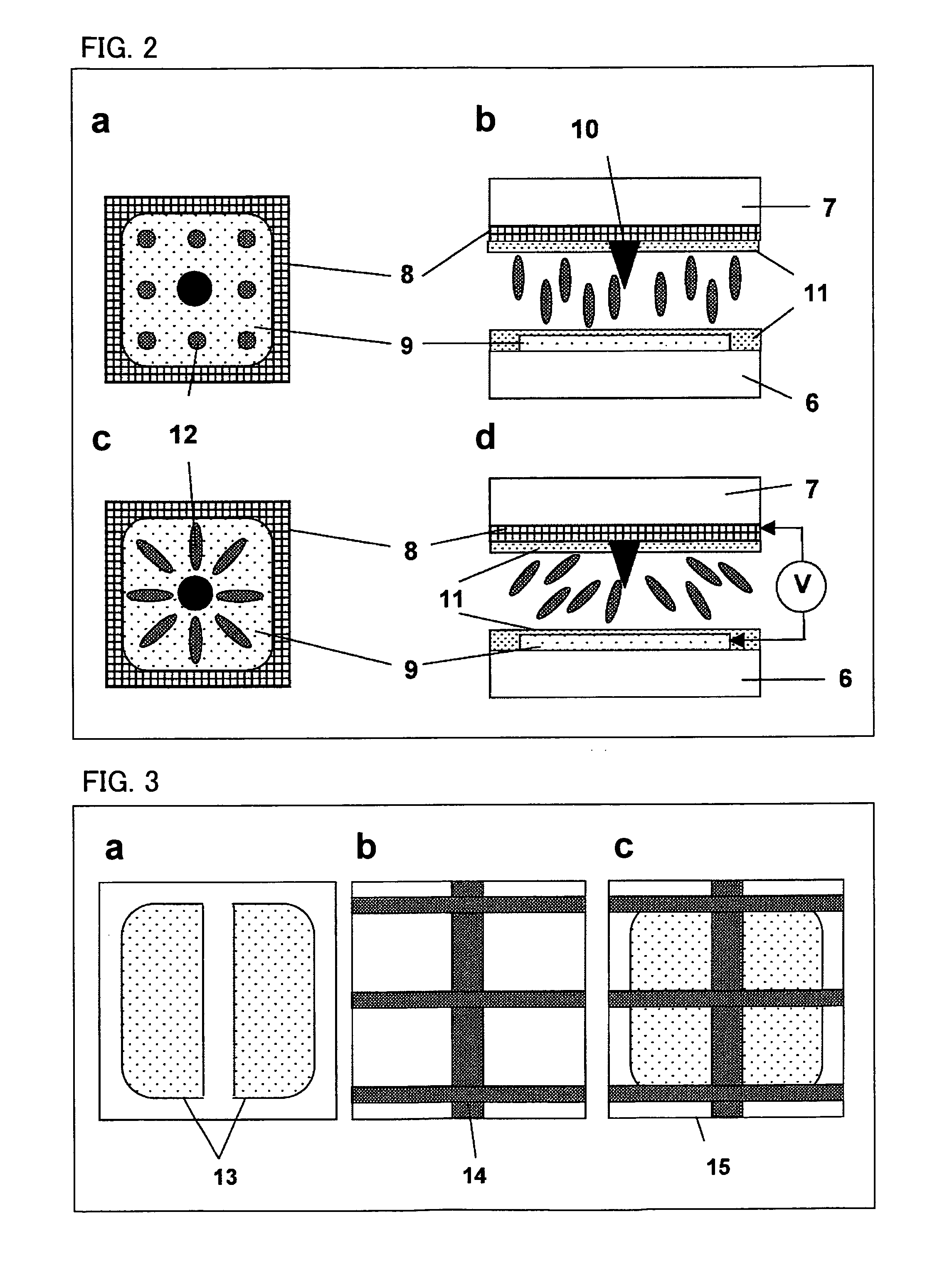
[0081]In a preferred embodiment of the invention, the LCD is a vertically aligned nematic (VAN) type LCD operating in an advanced super view mode (ASV) whereby the sub-pixel display elements are comprised of one or more continuous pinwheel alignment (CPA) domains, which are typically 30-100 μm square.

[0082]FIGS. 2a to 2d are schematic diagrams of a liquid crystal cell or pixel region forming part of a liquid crystal device comprising an array of such cells or regions. FIGS. 2a to 2d show a standard CPA domain viewed from above the LC cell (FIG. 2a) and as a slice through the cell (FIG. 2b) at zero applied voltage, and with a voltage applied between electrodes disposed on the inner surfaces of the opposing glass substrates (FIGS. 2c and 2d). The ASV type display comprises a lower active matrix glass substrate 6 and a counter substrate 7 opposed to each other with a predetermined separation. The counter substrate is coated with a transparent electrode material such as Indium Tin Oxide...


PUM

PropertyMeasurementUnit
thicknessaaaaaaaaaa
thicknessaaaaaaaaaa
voltagesaaaaaaaaaa

Abstract

A liquid crystal device comprises an active matrix substrate (6) and a counter-substrate (7) provided with homeotropic alignment surfaces (11). A layer of nematic liquid crystal material is provided between the alignment surfaces (11) so as to form a vertically aligned nematic device. The substrates (6, 7) carry a pixel electrode arrangement and a counter-electrode arrangement which define a plurality of pixel regions. Each of least some of these regions has a pixel electrode (13), which may be split into two halves, and a counter-electrode (8) which are arranged to apply an electric field for controlling the liquid crystal director (12) out-of-plane tilt angle. A further electrode (14), for example in the form of a plurality of parallel fingers, cooperates with at least one of the other electrodes (8, 13) to apply a second electric field for controlling the director in-plane azimuth angle. Such a device may be used, for example, as a switchable public / private display.

Description

TECHNICAL FIELD[0001]The present invention relates to a liquid crystal (LC) device. Examples of such a device may have public and private viewing modes. In typical examples of such a device used as a display, a single LC layer is used to display an image, the same LC layer being switchable between two states, one of which provides a wide range of viewing angles for said image, the other providing a restricted range of angles from which the displayed image can be observed.[0002]The term “LCD” is used herein to mean a liquid crystal device or a liquid crystal display according to the context.BACKGROUND ART[0003]Electronic display devices, such as monitors used with computers and screens built in to telephones and portable information devices, are usually designed to have a viewing angle as wide as possible, so that they can be read from any viewing position. However, there are some situations where a display that is visible from only a narrow range of angles is useful. For example, on...

Claims


Application Information

Patent Timeline
Patent Type & Authority Patents(United States)
IPC IPC(8): G02F1/1343G02F1/13G02F1/139G09G3/34G02F1/1337
CPCG02F1/1393G02F2001/134381G02F1/133707G02F1/134309G02F1/1323G02F2001/133776G02F1/133776G02F1/134381
Inventor BROUGHTON, BENJAMIN JOHNSMITH, NATHAN JAMESEVANS, ALLANGASS, PAUL ANTONY
Owner SHARP KK
Why Eureka
Try Eureka