System and method for automatically reconfiguring chain of abutted devices in electronic circuit design

a technology of electronic circuit design and automatic reconfiguration, which is applied in the direction of software simulation/interpretation/emulation, instruments, program control, etc., can solve the problems of difficult identification of individual devices, increased complexity of circuit design, and increased time and effort of design teams

Active Publication Date: 2014-12-09
CADENCE DESIGN SYST INC
View PDF6 Cites 20 Cited by
  • Summary
  • Abstract
  • Description
  • Claims
  • Application Information

AI Technical Summary

Problems solved by technology

As circuit complexity and transistor counts continue to exponentially grow, circuit design becomes much more challenging and demanding.
For circuit designers to successfully insert, modify, interconnect, and remove devices such as transistors into complex functional structures such as logic arrays, chains, and the like to fit within a circuit design, design teams have to expend substantial time and effort.
In chains of greater numbers of devices, identification of individual devices may be difficult as portions may be communally shared on multiple sides with other devices.
When a change is made to a circuit design, there is a risk of a designer inadvertently introducing mistakes—the remedy for which may require additional unnecessary design flow iterations from design to verification and back.
In a system with great numbers of transistors arranged in intricate and integral functional structures, even a minor mistake may have significant adverse impact on the operation of the given circuit.
Worse yet, if the mistake is not detected and properly remedied by verification systems, a defective integrated circuit product may be fabricated.
In systems heretofore known for circuit design, where a pre-established chain of interconnected devices in a circuit design requires the intermediate insertion of another device or chain, a designer must perform a number of time-consuming and error-prone operations beginning with manually initiating deconstruction of the devices from the chain.
This is all the more difficult in a chain of mutually abutted devices with neighboring devices sharing overlapping portions.
Such approach is not efficient and unduly prone to error.

Method used


Image

  • System and method for automatically reconfiguring chain of abutted devices in electronic circuit design
  • System and method for automatically reconfiguring chain of abutted devices in electronic circuit design
  • System and method for automatically reconfiguring chain of abutted devices in electronic circuit design

Examples


Embodiment Construction

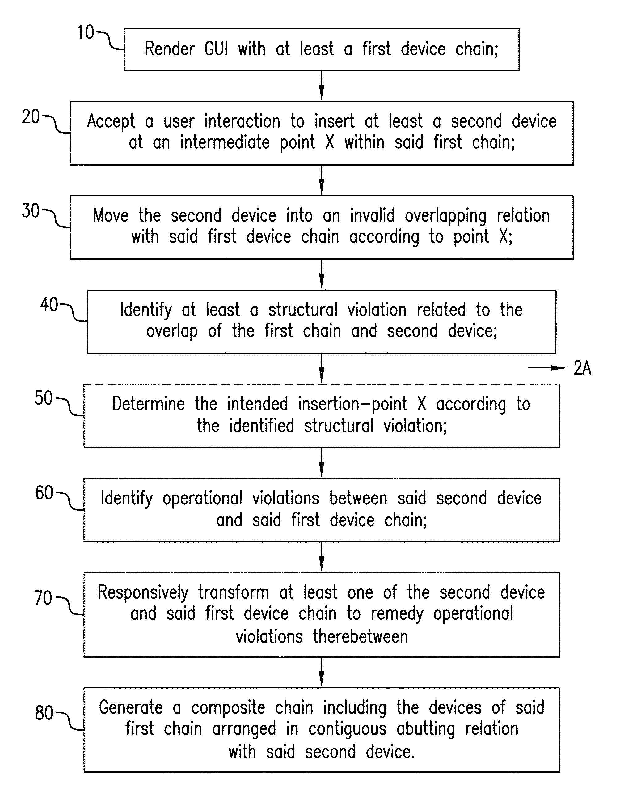
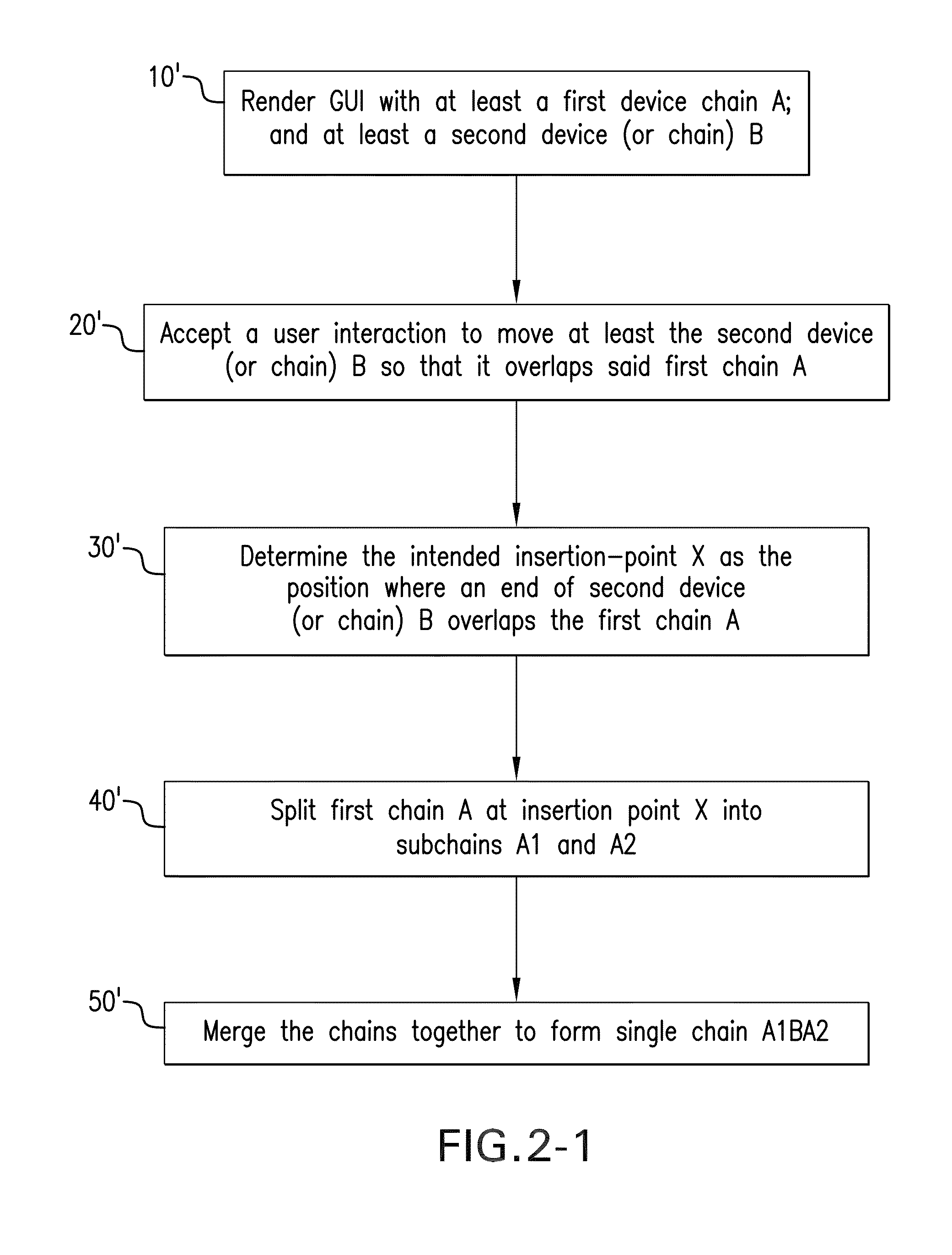
[0024]The subject system and method are generally directed to the highly automated insertion of at least one device, and optionally a chain of devices (or chains of devices), into a given chain (or chains) of interconnected devices within a graphical representation of a circuit design such as a circuit layout, circuit mask, circuit schematic, or the like. In a typical application, the given device chain (denoted ‘pre-existing’ for convenient reference purposes) and an additional device or chain to be inserted are selectively identified by a user, along with general indication of where on the pre-existing chain the insertion is desired. The system and method then automatically actuate the intervening processes necessary to effect the insertion, and thereby reconfigure the pre-existing chain of devices accordingly. For example, the system and method automatically determines one or more appropriate insertion points on the pre-existing device chain at the generally indicated region for ...


PUM


Abstract

The subject system and method are generally directed to the user-friendly insertion of at least one device, and optionally chains of devices, into at least one pre-existing chain of interconnected devices within a graphical representation of a circuit design such as a circuit layout, circuit mask, or a schematic. The system and method provide for discerning the intended insertion points and performing remedial transformations of the devices within the chains to ensure compliance with both structural and operational requirements of the circuit design.

Description

BACKGROUND OF THE INVENTION[0001]The present invention is generally directed to a system and method for automatic reconfiguration of a chain of interconnected devices within an electronic circuit design. More specifically, a system and method are provided for user-friendly insertion of at least one device, and optionally a chain (or chains) of devices, into a pre-existing chain (or chains) of interconnected devices within a graphical representation of a circuit design such as a circuit layout, circuit mask, circuit schematic, or the like within an electronic design automation (EDA) tool in rule-compliant manner.[0002]Presently, a given circuit design may incorporate upwards of tens of billions of transistors or more. Moore's law has established a timeline of a doubling of transistors in a given Integrated Circuit (IC) product-line every 18 months. As circuit complexity and transistor counts continue to exponentially grow, circuit design becomes much more challenging and demanding. F...

Claims


Application Information

Patent Timeline
Patent Type & Authority Patents(United States)
IPC IPC(8): G06F9/455G06F17/50
CPCG06F17/5081G06F17/5072G06F30/392
Inventor WILSON, THOMASGINETTI, ARNOLDFERGUSON, KENNETHPEI, YUAN-KAI
Owner CADENCE DESIGN SYST INC
Why Eureka
Try Eureka