Semiconductor light emitting device and method for manufacturing the same

a technology of semiconductor, which is applied in the direction of semiconductor/solid-state device manufacturing, semiconductor devices, and electrical equipment, etc., can solve the problems of deterioration of light efficiency in the semiconductor light emitting device package, loss of light, and indium content, so as to reduce contact resistance and improve current injection efficiency

Inactive Publication Date: 2014-12-16
LG DISPLAY CO LTD
View PDF9 Cites 5 Cited by
  • Summary
  • Abstract
  • Description
  • Claims
  • Application Information

AI Technical Summary

Benefits of technology

[0012]An advantage of the present invention is to provide a semiconductor light emitting device and a method for manufacturing that same, in which the semiconductor light emitting device includes a light transmissive electrode layer formed using a conductive thin film and an insulating thin film to substitute for a transparent electrode layer.
[0013]Another advantage of the present invention is to provide a semiconductor light emitting device and a method for manufacturing that same, in which a contact area between a metal electrode and a conductive thin film constituting a light transmissive electrode layer can be increased to reduce contact resistance between the light transmissive electrode layer and the metal electrode and improve current injection efficiency.
[0014]Other advantage of the present invention is to provide a semiconductor light emitting device and a method for manufacturing that same, in which characteristic variation of a conductive thin film constituting a light transmissive electrode layer can be minimized.
[0015]Additional advantages and features of the invention will be set forth in part in the description which follows and in part will become apparent to those having ordinary skill in the art upon examination of the following or may be learned from practice of the invention. The objectives and other advantages of the invention may be realized and attained by the structure particularly pointed out in the written description and claims hereof as well as the appended drawings.
[0016]To achieve these objects and other advantages and in accordance with the purpose of the invention, as embodied and broadly described herein, a semiconductor light emitting device according to one aspect of the present invention comprises a substrate; a first semiconductor layer formed on the substrate; an active layer formed on the first semiconductor layer; a second semiconductor layer formed on the active layer; a light transmissive electrode layer formed on the second semiconductor layer, the light transmissive electrode layer having a structure in which at least one conductive thin film and at least one insulating thin film are deposited; and a first electrode formed on the light transmissive electrode layer, wherein the light transmissve electrode layer includes at least one contact portion for contacting the at least one conductive thin film with the first electrode.
[0017]In another aspect of the present invention, a method for manufacturing a semiconductor light emitting device comprises the steps of forming a first semiconductor layer on a substrate; forming an active layer on the first semiconductor layer; forming a second semiconductor layer on the active layer; partially etching the active layer and the second semiconductor layer until the first semiconductor layer is exposed; heating the substrate on which the first semiconductor layer, the active layer and the second semiconductor layer are formed; and forming a light transmissive electrode layer on the second semiconductor layer, the light transmissive electrode layer including at least one conductive thin film and at least one insulating thin film.

Problems solved by technology

However, problems occur in that the ITO is expensive and contains indium, which is a rare metal and thus may be exhausted later.
Also, if the transparent electrode layer 170 is formed using the ITO, since light transmittance of the ITO is more than 90%, light may re-enter the light emitting device due to scattering with a phosphor or other material included in the light emitting device package, whereby the light may be lost.
For this reason, a problem occurs in that light efficiency may be deteriorated in the semiconductor light emitting device package.

Method used


Image

  • Semiconductor light emitting device and method for manufacturing the same
  • Semiconductor light emitting device and method for manufacturing the same
  • Semiconductor light emitting device and method for manufacturing the same

Examples


first embodiment

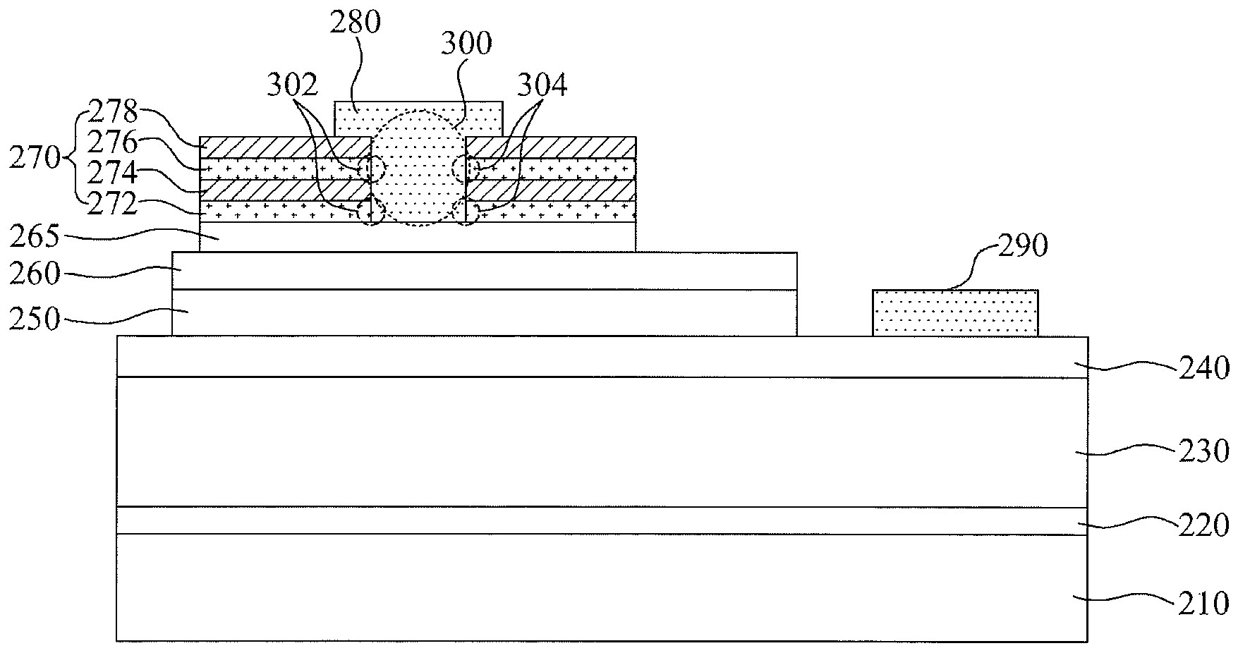
[0069]At this time, a contact portion 300 as shown in FIG. 7, may be formed by partially etching the first conductive thin film 272, the first insulating thin film 274, the second conductive thin film 276, and the second insulating thin film 278 until the second semiconductor layer 260 is exposed.

[0070]According to this embodiment, the P type electrode 280 may be formed on a region that covers one or more contact portions 300 on the light transmissive electrode layer 270 as well as the inside of the one or more contact portions 300.

[0071]As a result, the P type electrode 280 is in contact with sidewalls 302 and 304 of the first and second conductive thin films 272 and 276 constituting the light transmissive electrode layer 270, whereby contact resistance and current injection efficiency may be improved, and current crowding may be prevented from occurring. In this way, electric characteristics of the semiconductor light emitting device 200 may be improved.

second embodiment

[0072]A contact portion 310 as shown in FIG. 8, may be formed by partially etching the first insulating thin film 274, the second conductive thin film 276, and the second insulating thin film 278 until the first conductive thin film 272 is exposed.

[0073]According to this embodiment, the P type electrode 280 may be formed on a region that covers one or more contact portions 310 on the light transmissive electrode layer 270 as well as the inside of the one or more contact portions 310.

[0074]As a result, since the P type electrode 280 is in contact with a surface 314 of the first conductive thin film 272 as well as a sidewall 312 of the second conductive thin film 276 constituting the light transmissive electrode layer 270, the contact region may be more extended than that of the first embodiment, whereby current crowding may be more reduced.

[0075]Hereinafter, a method for manufacturing a semiconductor light emitting device according to the present invention will be described with ref...


PUM


Abstract

A semiconductor light emitting device, which includes a light transmissive electrode layer formed using a conductive thin film and an insulating thin film to substitute for a transparent electrode layer, comprises a substrate; a first semiconductor layer formed on the substrate; an active layer formed on the first semiconductor layer; a second semiconductor layer formed on the active layer; a light transmissive electrode layer formed on the second semiconductor layer, the light transmissive electrode layer having a structure in which at least one conductive thin film and at least one insulating thin film are deposited; and a first electrode formed on the light transmissive electrode layer, wherein the light transmissve electrode layer includes at least one contact portion for contacting the at least one conductive thin film with the first electrode.

Description

CROSS REFERENCE TO RELATED APPLICATIONS[0001]This application claims the benefit of the Korean Patent Application No. 10-2011-0081548 filed on Aug. 17, 2011, which is hereby incorporated by reference for all purposes as if fully set forth herein.BACKGROUND OF THE INVENTION[0002]1. Field of the Invention[0003]The present invention relates to a semiconductor device, and more particularly, to a semiconductor light emitting device.[0004]2. Discussion of the Related Art[0005]Generally, a semiconductor light emitting device has a light emitting region containing ultraviolet, blue, and green regions. In particular, a GaN-based semiconductor light emitting device may be used for an optical device of a blue / green light emitting diode (LED), and an electronic device with high speed switching and high output power performance such as a metal semiconductor field effect transistor (MESFET), a hetero junction field effect transistor (HEMT), etc.[0006]FIG. 1 is a perspective view illustrating a st...

Claims


Application Information

Patent Timeline
Patent Type & Authority Patents(United States)
IPC IPC(8): H01L33/20H01L33/42
CPCH01L33/42H01L33/20H01L33/36H01L33/38
Inventor JUNG, TAEILKIM, YOUNGCHAEKIM, SUNMANHAN, YEJIPARK, CHUNGHOONCHOI, BYEONG-KYUNKANG, SE-EUN
Owner LG DISPLAY CO LTD
Why Eureka
Try Eureka