Methods for forming a round bottom silicon trench recess for semiconductor applications

a technology of semiconductor fabrication and trench recess, which is applied in the direction of semiconductor devices, electrical equipment, electric discharge tubes, etc., can solve the problems of short channel, increase the off-current threshold, and deteriorate the refresh characteristics

Active Publication Date: 2015-01-13
APPLIED MATERIALS INC
View PDF24 Cites 90 Cited by
  • Summary
  • Abstract
  • Description
  • Claims
  • Application Information

AI Technical Summary

Problems solved by technology

However, as the miniaturization of circuit technology is pressed, the shrinking dimensions of interconnects in VLSI and ULSI technology have placed additional demands on the processing capabilities.
Decreased channel length may result in short channel effects, which may increase an off-current threshold of the transistors ad can deteriorate refresh characteristics of memory devices having such transistors.
However, formation of such shapes or features often require complicated and multiple process steps to complete the manufacture process, resulting in increases of manufacturing cycle time and cost with decreased process throughput.
Furthermore, poor etching selectivity and control occurring during manufacturing processes for such shapes or features in the recess channels may undesirably result in an inaccurate profile control, thereby eventually leading to device failure.

Method used


Image

  • Methods for forming a round bottom silicon trench recess for semiconductor applications
  • Methods for forming a round bottom silicon trench recess for semiconductor applications
  • Methods for forming a round bottom silicon trench recess for semiconductor applications

Examples


Embodiment Construction

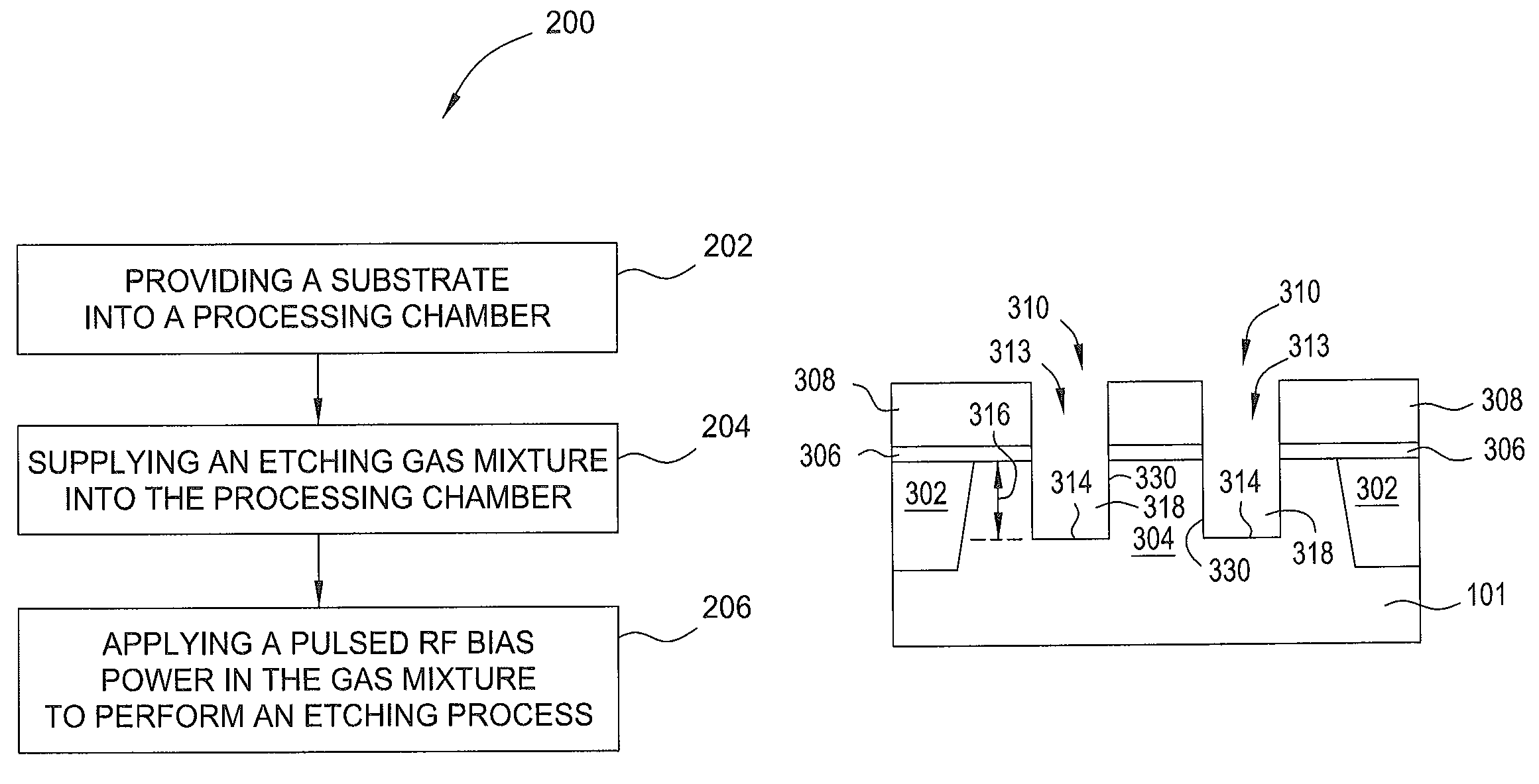
[0018]The present invention provides a method and apparatus for manufacturing a recess channel structure in a semiconductor substrate. More specifically, the invention relates to methods of utilizing a single etching step to manufacture a recess channel structure in a semiconductor substrate in semiconductor device applications. In one embodiment, the recess channel structure with a round bottom feature, e.g., a spherical-like structure, formed at a bottom of a trench is formed by using a single etching step to etch a silicon material defining the semiconductor substrate. The single etching step utilizes a pulsed RF bias power mode to incrementally etch the round bottom feature at the bottom of the trench, thereby forming a channel recess with round bottom feature, e.g., a spherical-like structure, in the semiconductor substrate.

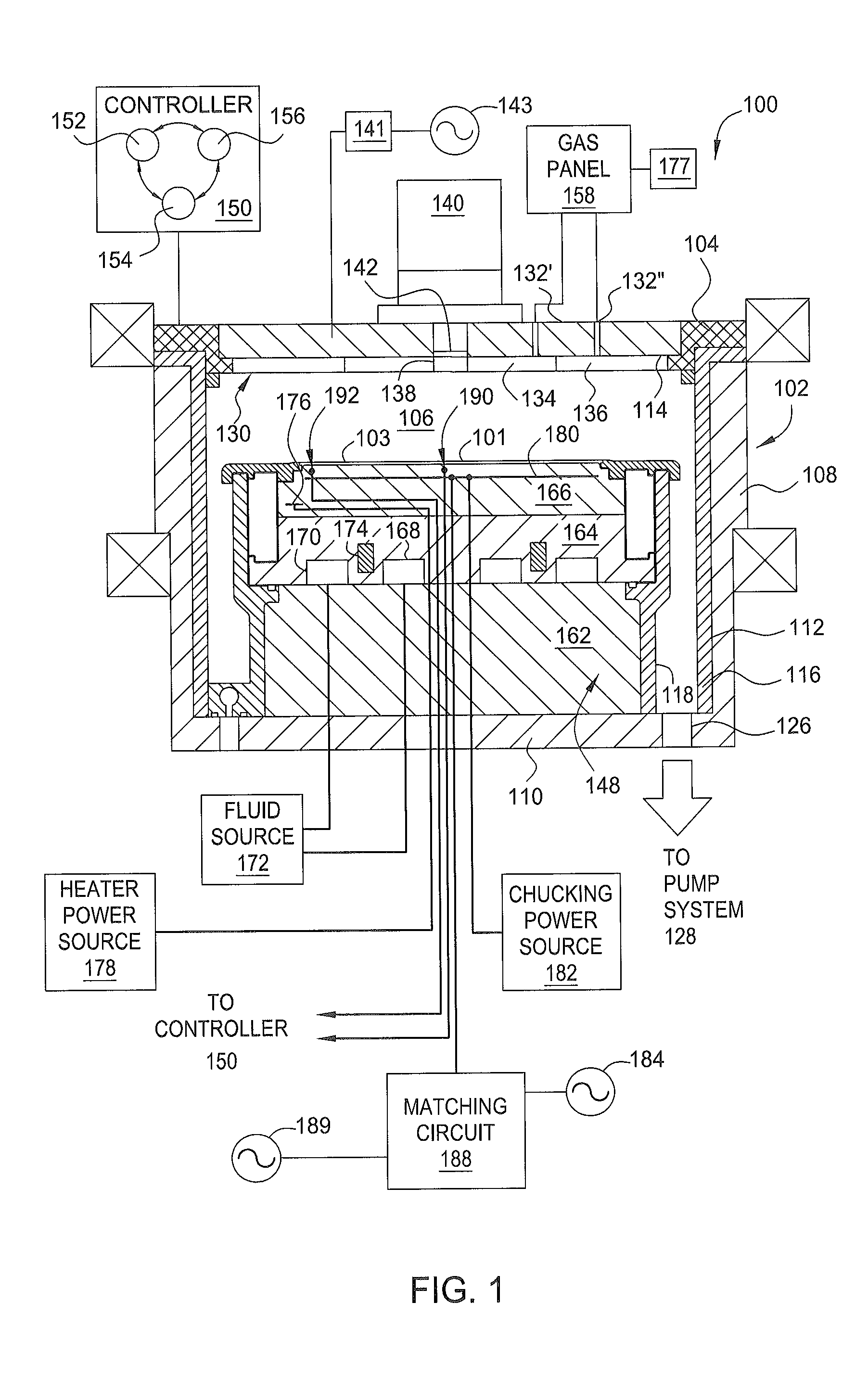
[0019]FIG. 1 is a sectional view of one embodiment of a processing chamber 100 suitable for manufacturing a recess channel structure in a semiconductor subs...


PUM


Abstract

Embodiments of the present invention provide methods to etching a recess channel in a semiconductor substrate, for example, a silicon containing material. In one embodiment, a method of forming a recess structure in a semiconductor substrate includes transferring a silicon substrate into a processing chamber having a patterned photoresist layer disposed thereon exposing a portion of the substrate, providing an etching gas mixture including a halogen containing gas and a Cl2 gas into the processing chamber, supplying a RF source power to form a plasma from the etching gas mixture, supplying a pulsed RF bias power in the etching gas mixture, and etching the portion of the silicon substrate exposed through the patterned photoresist layer in the presence of the plasma.

Description

BACKGROUND[0001]1. Field[0002]Embodiments of the present invention generally relate to a method for forming a round bottom silicon trench recess, more specifically, to a method for forming a round bottom silicon trench recess in semiconductor fabrication applications.[0003]2. Description of the Related Art[0004]Reliably producing submicron and smaller features is one of the key technologies for the next generation of very large scale integration (VLSI) and ultra large scale integration (ULSI) of semiconductor devices. However, as the miniaturization of circuit technology is pressed, the shrinking dimensions of interconnects in VLSI and ULSI technology have placed additional demands on the processing capabilities. The multilevel interconnects that lie at the heart of this technology require precise processing of high aspect ratio features, such as vias and other interconnects. Reliable formation of these interconnects is very important to VLSI and ULSI success and to the continued ef...

Claims


Application Information

Patent Timeline
Patent Type & Authority Patents(United States)
IPC IPC(8): H01L21/302H01L21/3065H01L21/311H01L21/762H01L21/768
CPCH01L21/762H01L21/76898H01L21/31116H01L21/30655H01L21/3065H01J37/32082H01J2237/3347H01L21/67109H01L21/6831H01L21/76224H01L29/66621
Inventor HAN, JOO WONCHO, KEE YOUNGCHO, HAN SOOKIM, SANG WOOKKHAN, ANISUL H.
Owner APPLIED MATERIALS INC
Why Eureka
Try Eureka