Array substrate for liquid crystal display and method for manufacturing the same

a liquid crystal display and substrate technology, applied in non-linear optics, instruments, optics, etc., can solve problems such as poor viewing angle characteristics, and achieve the effect of reducing the surface area of contact holes and improving transmittan

Active Publication Date: 2015-01-13
LG DISPLAY CO LTD
View PDF6 Cites 5 Cited by
  • Summary
  • Abstract
  • Description
  • Claims
  • Application Information

AI Technical Summary

Benefits of technology

[0009]Embodiments of the present invention have been made in an effort to provide an array substrate for a liquid crystal display, which improves transmittance by reducing the surface area of a contact hole, and may solve problems concerning the non-spreading of an alignment film, and a method for manufacturing the same.

Problems solved by technology

However, the driving of liquid crystal by the vertically applied electric field is disadvantageous in that viewing angle characteristics are not good.
However, the depth of a contact hole that connects the thin film transistor and the pixel electrode is quite large, and hence the alignment film may not be spread into the contact hole.
However, because an interval between the nozzles of the inkjet device is wide, an ink emitted from the nozzle is not widely spread on the alignment layer 30 and thus is not filled in a contact hole.

Method used


Image

  • Array substrate for liquid crystal display and method for manufacturing the same
  • Array substrate for liquid crystal display and method for manufacturing the same
  • Array substrate for liquid crystal display and method for manufacturing the same

Examples


Embodiment Construction

[0022]Reference will now be made in detail to embodiments of the invention, examples of which are illustrated in the accompanying drawings. Wherever possible, the same reference numbers will be used throughout the drawings to refer to the same or like parts.

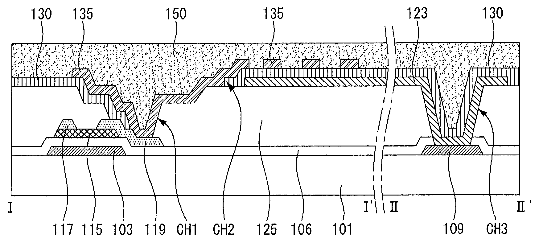
[0023]FIG. 3 is a top plan view showing an array substrate for a liquid crystal display in accordance with an exemplary embodiment of the present invention.

[0024]Referring to FIG. 3, a gate line 103 is positioned on a substrate (not shown) comprising a plurality of subpixels P so as to extend in one direction, and a data line 107 that crosses the gate line 103. A common line 109 is arranged parallel to the gate line 103, and crosses the data line 107. The subpixel P shown in FIG. 3 is defined by the crossings of the gate line 103, the data line 107, and the common line 109.

[0025]A thin film transistor Tr is positioned in a subpixel P, and comprises a gate electrode (not shown) connected to the gate line 103, a gate insulating fil...


PUM

PropertyMeasurementUnit
insulatingaaaaaaaaaa
optical anisotropyaaaaaaaaaa
electric fieldaaaaaaaaaa

Abstract

An array substrate for a liquid crystal display and a method for manufacturing the same are disclosed. The array substrate for a liquid crystal display includes a source electrode and a drain electrode and an organic insulating film positioned on the source electrode and the drain electrode. The organic insulating layer includes a first contact hole exposing the drain electrode, and having a stepped level difference formed on the sloping surface of the first contact hole.

Description

[0001]This application claims the benefit of priority of Korean Patent Application No. 10-2012-0055445 filed on May 24, 2012, the entire contents of which are incorporated herein by reference for all purposes as if fully set forth herein.FIELD OF THE INVENTION[0002]This disclosure relates to an array substrate for a liquid crystal display and a method for manufacturing the same. This disclosure also relates to an array substrate for a liquid crystal display which prevents defective application of an alignment film and improves display quality by forming a level difference in a contact hole, and a method for manufacturing the same.DISCUSSION OF THE RELATED ART[0003]In general, a liquid crystal display utilizes optical anisotropy and polarization properties of a liquid crystal. Liquid crystals have a thin, long structure, and have an orientation in the alignment of their molecules. The direction of the alignment of liquid crystal molecules can be controlled by applying an electric fie...

Claims


Application Information

Patent Timeline
Patent Type & Authority Patents(United States)
IPC IPC(8): H01L29/04G02F1/1337G02F1/1343G02F1/1362H01L27/12
CPCG02F1/136227H01L27/124H01L27/1288H01L27/1248G02F1/133711G02F2001/134372G02F1/134372G02F1/1343G02F1/136
Inventor KIM, JINPILJUNG, KIYOUNGMIN, KEUMKYUJANG, SANGSU
Owner LG DISPLAY CO LTD
Why Eureka
Try Eureka