Heat spreading substrate with embedded interconnects

a technology of embedded interconnects and heat spreading substrates, which is applied in the direction of semiconductor devices, semiconductor/solid-state device details, electrical apparatus, etc., can solve the problems of ineffective cost effective removal of heat generated by such devices, sapphire or gallium arsenide (gaas), and poor conductivity of heat in the substrate of many such devices, so as to achieve simple and cost effective manufacturing

Active Publication Date: 2015-02-03
INVENSAS CORP
View PDF27 Cites 39 Cited by
  • Summary
  • Abstract
  • Description
  • Claims
  • Application Information

AI Technical Summary

Benefits of technology

[0003]Therefore, what is needed are systems and methods for heat spreading substrate with embedded interconnects. What is additionally needed are systems and methods for heat spreading substrate with embedded interconnects that are simple and cost effective to manufacture. A further need exists for systems and methods for heat spreading substrate with embedded interconnects that are compatible and complementary with existing systems and methods of integrated circuit design, manufacturing and test. Embodiments of the present invention provide these advantages.

Problems solved by technology

For example, many LED devices may be said to run “hot.” In addition, the substrates of many such devices, e.g., comprising sapphire or Gallium arsenide (GaAs), are not good conductors of heat.
Conventional mounting and heat sinking methods and structures do not cost effectively remove the heat generated by such devices.

Method used


Image

  • Heat spreading substrate with embedded interconnects
  • Heat spreading substrate with embedded interconnects
  • Heat spreading substrate with embedded interconnects

Examples


first embodiment

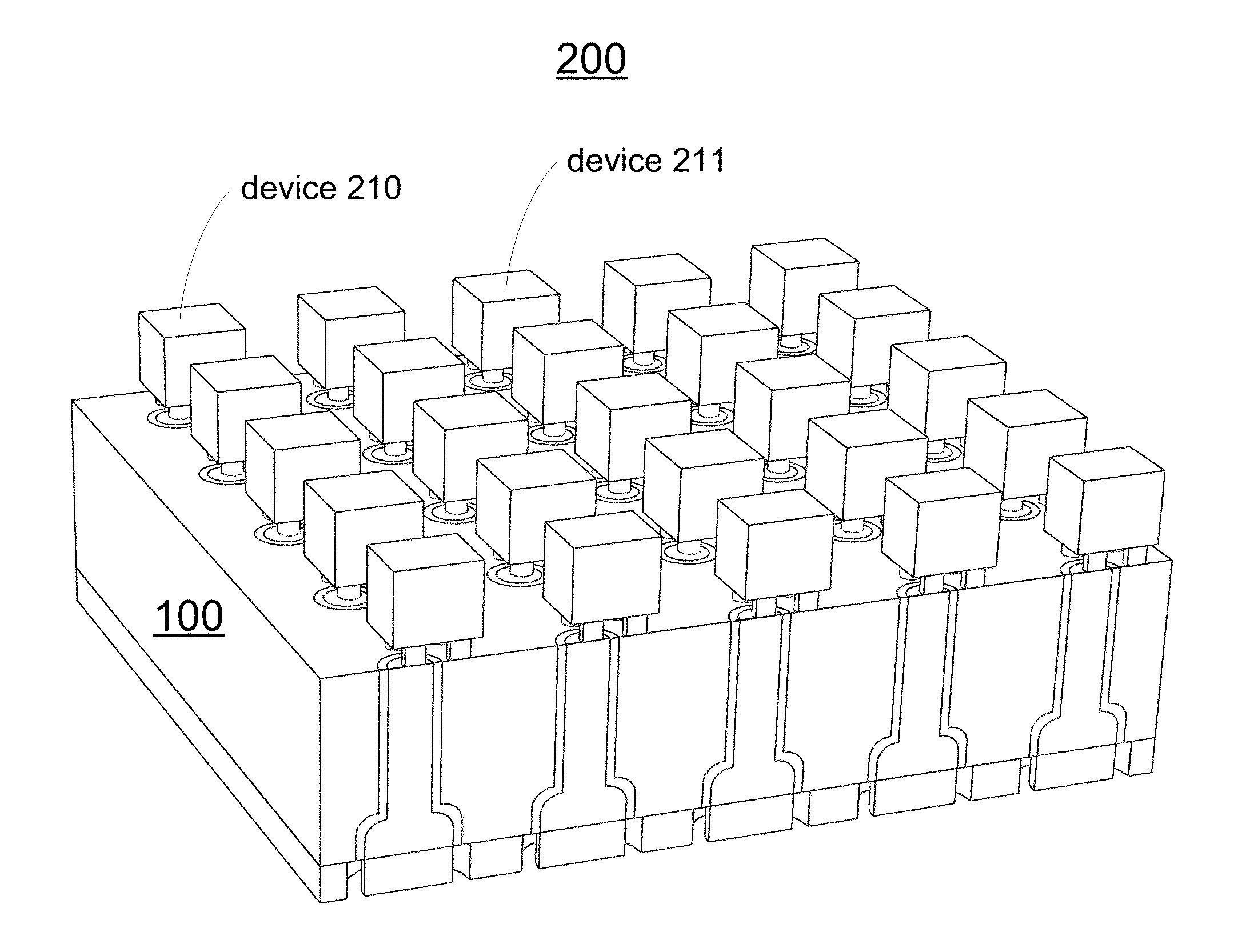
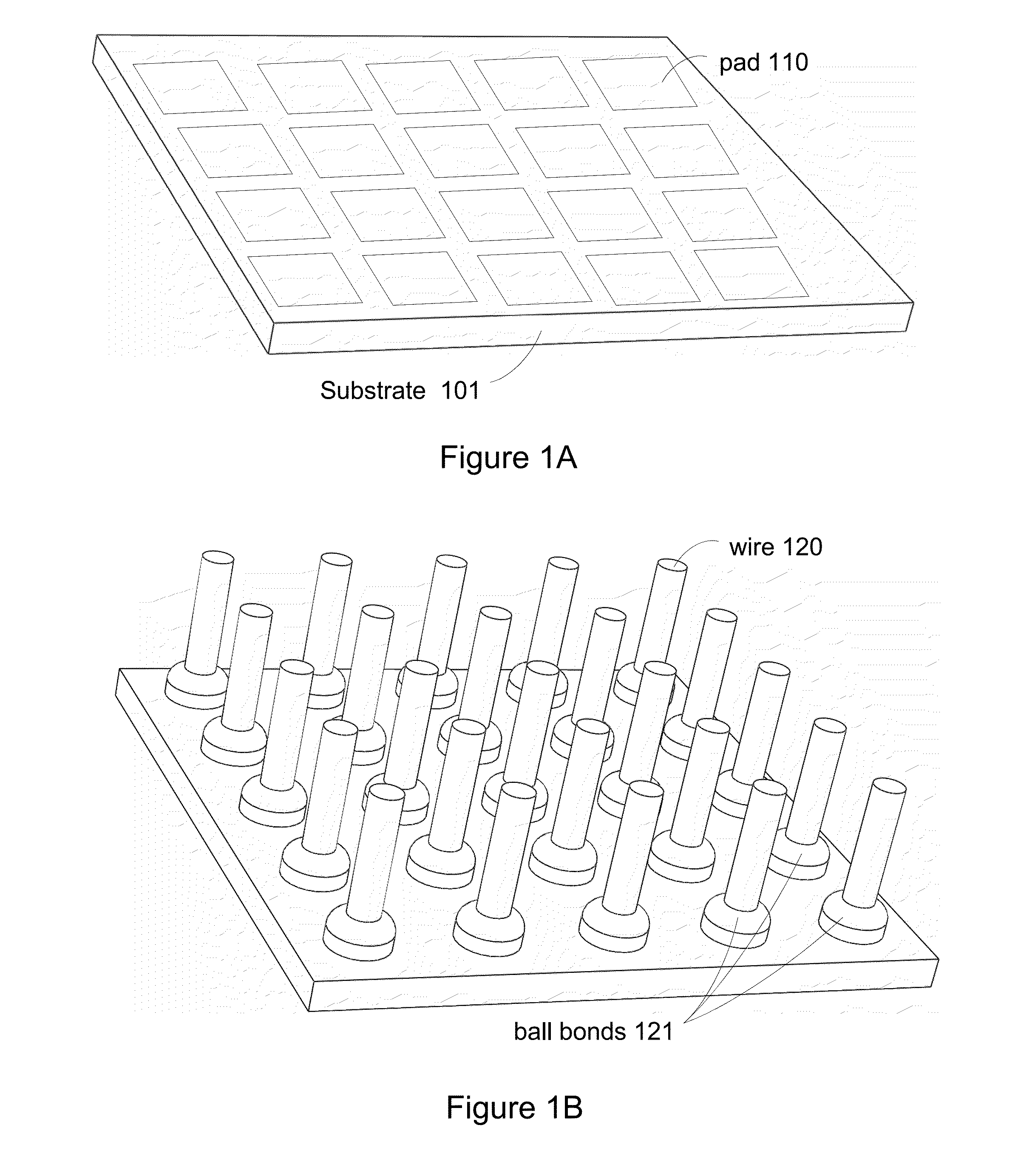
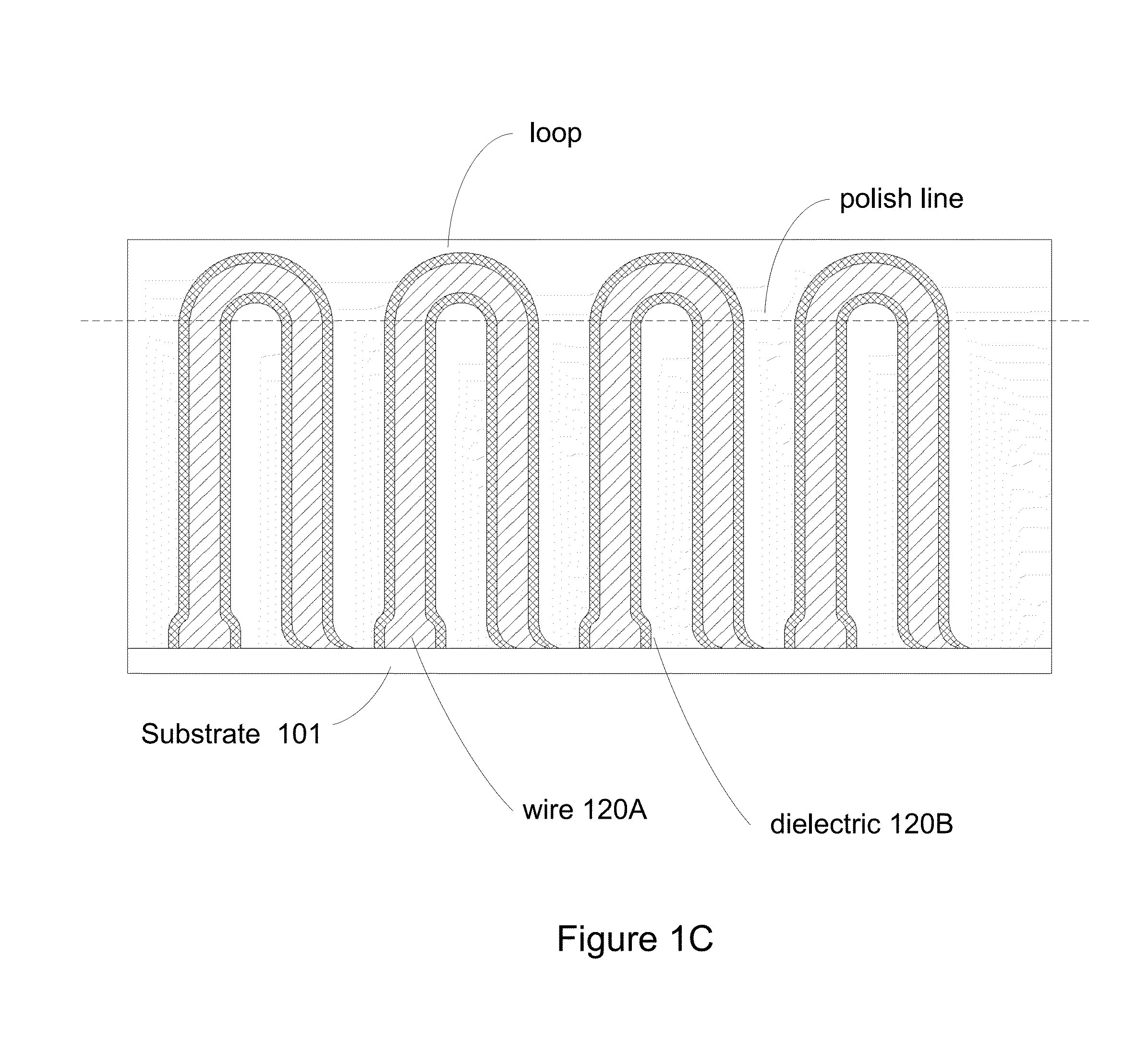
[0023]FIG. 1F illustrates a heat spreading substrate with embedded interconnects 100, in accordance with embodiments of the present invention. In FIG. 1F, the substrate 101 is optionally removed, in accordance with embodiments of the present invention. In addition, the top surface is optionally polished, exposing the conductive portion of the wire bond, 120A, exposed on both the top and bottom surfaces of metal 130. For example, if the wires 120A comprise loop bonding, top surface polishing may eliminate the loop in the wire, electrically isolating the remaining wires.

[0024]FIG. 1F also illustrates optional cut / polish extent line 107. In accordance with embodiments of the present invention, substrate 101 and / or metal 130 may be cut and / or polished to cut / polish line 107 to remove ball bonds 121. In this novel manner, the wires 120 may be placed closer together, e.g., without a need to physically separate ball bonds 121 from one another, and heat spreading substrate with embedded int...

second embodiment

[0025]FIG. 1G illustrates a heat spreading substrate with embedded interconnects 100, in accordance with embodiments of the present invention. In FIG. 1G, a substrate 101 comprising a metal film is optionally patterned to electrically isolate the wire bond pads 110, wires 120A and / or the ball bonds 121 from the metal 130. For example, a gap 135 is formed in film substrate 101.

third embodiment

[0026]FIG. 1H illustrates a heat spreading substrate with embedded interconnects 100, in accordance with embodiments of the present invention. FIG. 1H illustrates an alternative method of manufacture of heat spreading substrate with embedded interconnects 100, in accordance with embodiments of the present invention. Starting with the configuration of FIG. 1D, metal 131 is laminated to the substrate or film 101. Metal 131 comprises holes 132 that have been pre-drilled, perforated or otherwise formed. Holes 132 fit over wires 120 and ball bonds 121. After lamination of metal 131 to substrate 101, the remaining volume of the holes 132 may be filled in, e.g., plated.


PUM


Abstract

Heat spreading substrate with embedded interconnects. In an embodiment in accordance with the present invention, an apparatus includes a metal parallelepiped comprising a plurality of wires inside the metal parallelepiped. The plurality of wires have a different grain structure than the metal parallelepiped. The plurality of wires are electrically isolated from the metal parallelepiped. The plurality of wires may be electrically isolated from one another.

Description

FIELD OF INVENTION[0001]Embodiments of the present invention relate to the field of integrated circuit design and manufacture. More specifically, embodiments of the present invention relate to systems and methods for a heat spreading substrate with embedded interconnects.BACKGROUND[0002]A variety of semiconductor devices, for example, light emitting diodes (LED), radio frequency (RF) devices, motor controllers, power semiconductors and the like, may be characterized as having high power density. For example, many LED devices may be said to run “hot.” In addition, the substrates of many such devices, e.g., comprising sapphire or Gallium arsenide (GaAs), are not good conductors of heat. Conventional mounting and heat sinking methods and structures do not cost effectively remove the heat generated by such devices.SUMMARY OF THE INVENTION[0003]Therefore, what is needed are systems and methods for heat spreading substrate with embedded interconnects. What is additionally needed are syste...

Claims


Application Information

Patent Timeline
Patent Type & Authority Patents(United States)
IPC IPC(8): H01L33/00H01L23/36
CPCH01L23/142H01L21/486H01L24/97H01L2224/16225H01L2224/48091H01L2224/48472H01L2224/73265H01L2924/19107H01L2924/12041H01L2924/01322H01L2224/45139H01L2224/45124H01L2224/45144H01L2224/45147H01L2924/00011H01L2924/00014H01L2924/00H01L2924/01049H01L21/4875H01L23/14H01L21/4853H01L21/52H01L21/768H01L23/49568
Inventor MOHAMMED, ILYASBEROZ, MASUD
Owner INVENSAS CORP
Why Eureka
Try Eureka