Component-incorporated wiring substrate and method of manufacturing the same

a technology of component-incorporated wiring and wiring substrate, which is applied in the direction of final product manufacturing, sustainable manufacturing/processing, and semiconductor/solid-state device details. it can solve the problems of failure to ensure sufficient connection reliability between the built-in component and the via conductor, increase in dc resistance associated, and reduce the dc resistance associated with the connection between the first via conductor and the terminal electrode. it achieves a wide connection, and reduces the dc resistance resistan

Inactive Publication Date: 2015-02-10
NGK SPARK PLUG CO LTD
View PDF17 Cites 6 Cited by
  • Summary
  • Abstract
  • Description
  • Claims
  • Application Information

AI Technical Summary

Benefits of technology

[0008]The present invention has been conceived to solve the above problems, and an object of the invention is to provide a component-incorporated wiring substrate in which sufficient connection reliability is ensured in establishing connection of the built-in plate-like component by way of via conductors.
[0010]According to the component-incorporated wiring substrate of the present invention, the built-in plate-like component has the terminal electrode formed at an end with respect to the first direction, and the first via conductor has a tapered shape, extends through the insulation layer disposed on the side of the component corresponding to the main surface, and is electrically connected to the terminal electrode. In this case, the via diameter of the first via conductor as measured at the same level as that of the main surface of the terminal electrode is greater than the length of the main surface of the terminal electrode along the first direction. Thus, by means of the first via conductor being formed at an appropriate position, the first via conductor can be connected not only to the main surface of the terminal electrode but also to the side surface of the terminal electrode, whereby DC resistance can be reduced through sufficient increase in connection area. Also, in the process of manufacturing the component-incorporated wiring substrate, tolerance for positional deviation of the component increases, so that connection reliability can be improved.
[0011]The first via conductor of the present invention can be freely disposed, so long as it is connected to the side surface and the main surface of the terminal electrode. However, for example, as viewed in plane, a center axis of the first via conductor may coincide with the side surface. Through employment of such disposition, when positional deviation of the component along the first direction arises, a reduction in connection area between the first via conductor and the terminal electrode can be restrained to a relatively low level.
[0018]According to the present invention, since the first via conductor has a large via diameter, is formed for connection to the electrode terminal of a plate-like component incorporated in the wiring substrate, has a tapered shape, and is connected to both of the side surface and the main surface of the terminal electrode, there can be ensured a wide connection area which encompasses the area of connection to the side surface and the main surface of the terminal electrode. Therefore, DC resistance associated with connection between the first via conductor and the terminal electrode can be reduced, and large tolerance can be ensured for positional deviation of the component, whereby connection reliability can be enhanced in a comprehensive manner.

Problems solved by technology

Such a structure involves the following problem: in the manufacture of the wiring substrate, in a process of positioning the component in an accommodation hole, even a slight positional deviation may lead to a failure to maintain an electrical connection between the terminal electrodes and the via conductors.
Also, the above-mentioned structure encounters difficulty in securing a sufficient connection area between the terminal electrodes and the via conductors, potentially resulting in an increase in DC resistance associated with connection of the component to a power supply line.
As mentioned above, the conventional component-incorporated wiring substrate involves a problem of failure to ensure sufficient connection reliability between the built-in component and the via conductors.

Method used


Image

  • Component-incorporated wiring substrate and method of manufacturing the same
  • Component-incorporated wiring substrate and method of manufacturing the same
  • Component-incorporated wiring substrate and method of manufacturing the same

Examples


Embodiment Construction

[0032]A preferred embodiment of the present invention will next be described with reference to the drawings. However, the embodiment to be described below is a mere example of an application of the technical concept of the present invention. The contents of the embodiment should not be construed as limiting the invention.

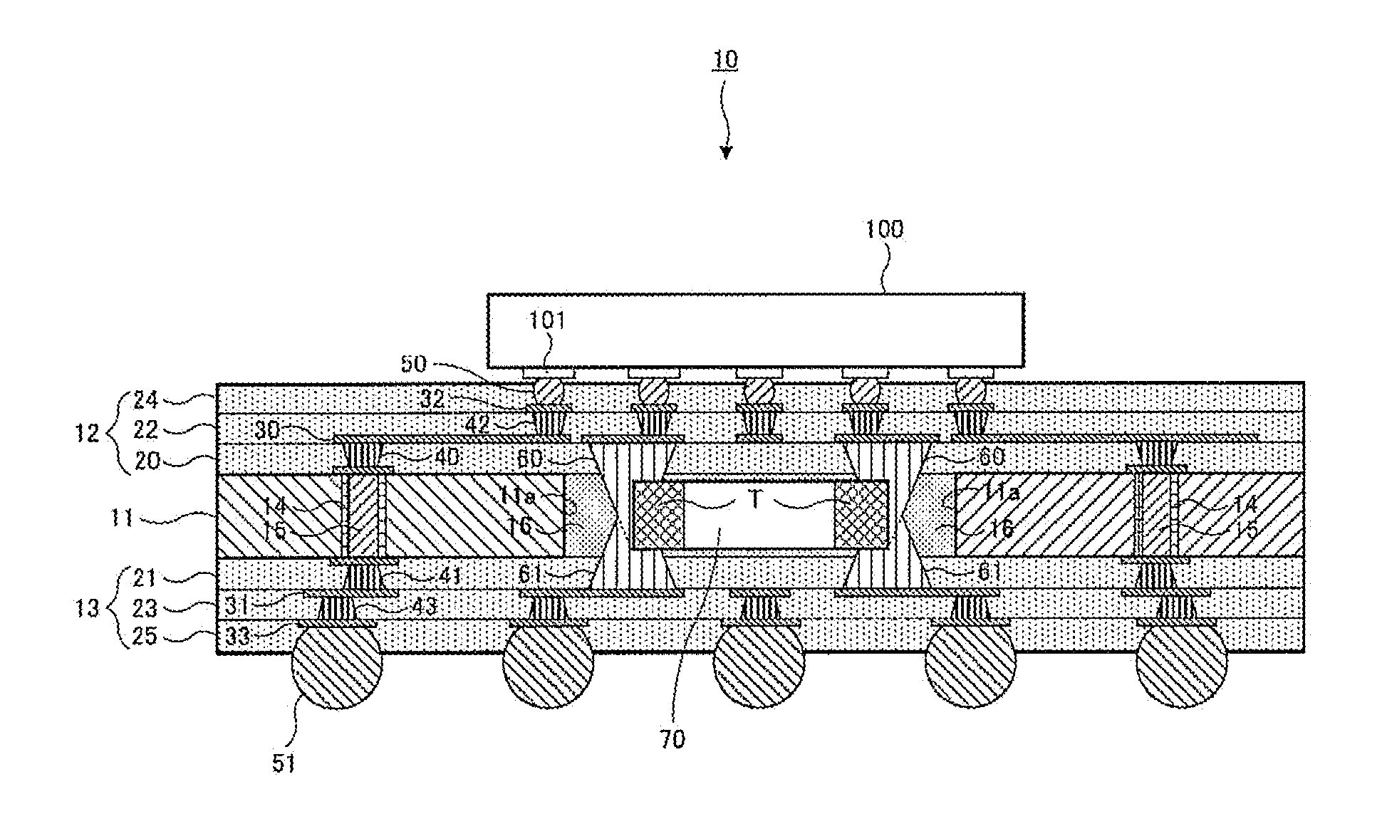
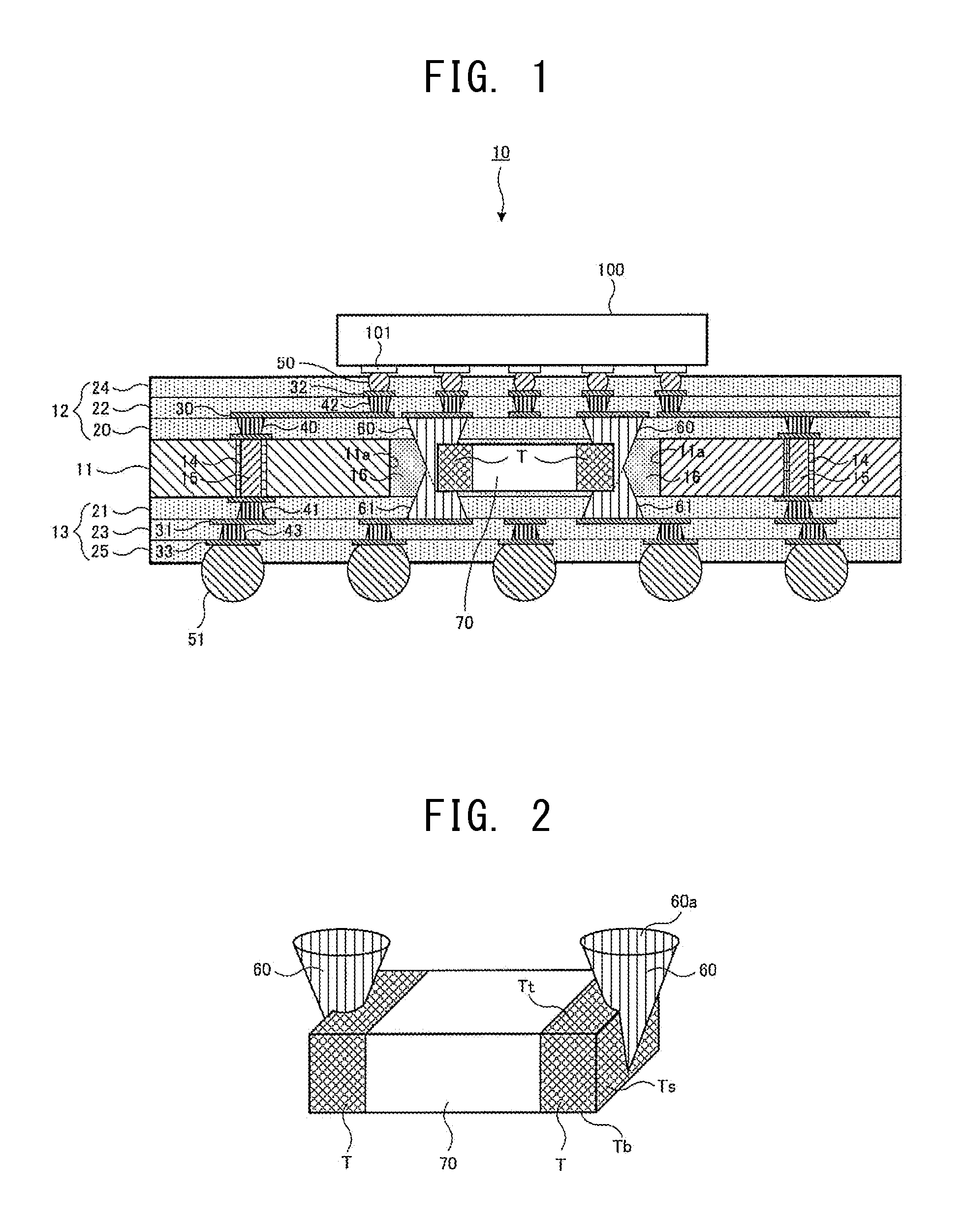
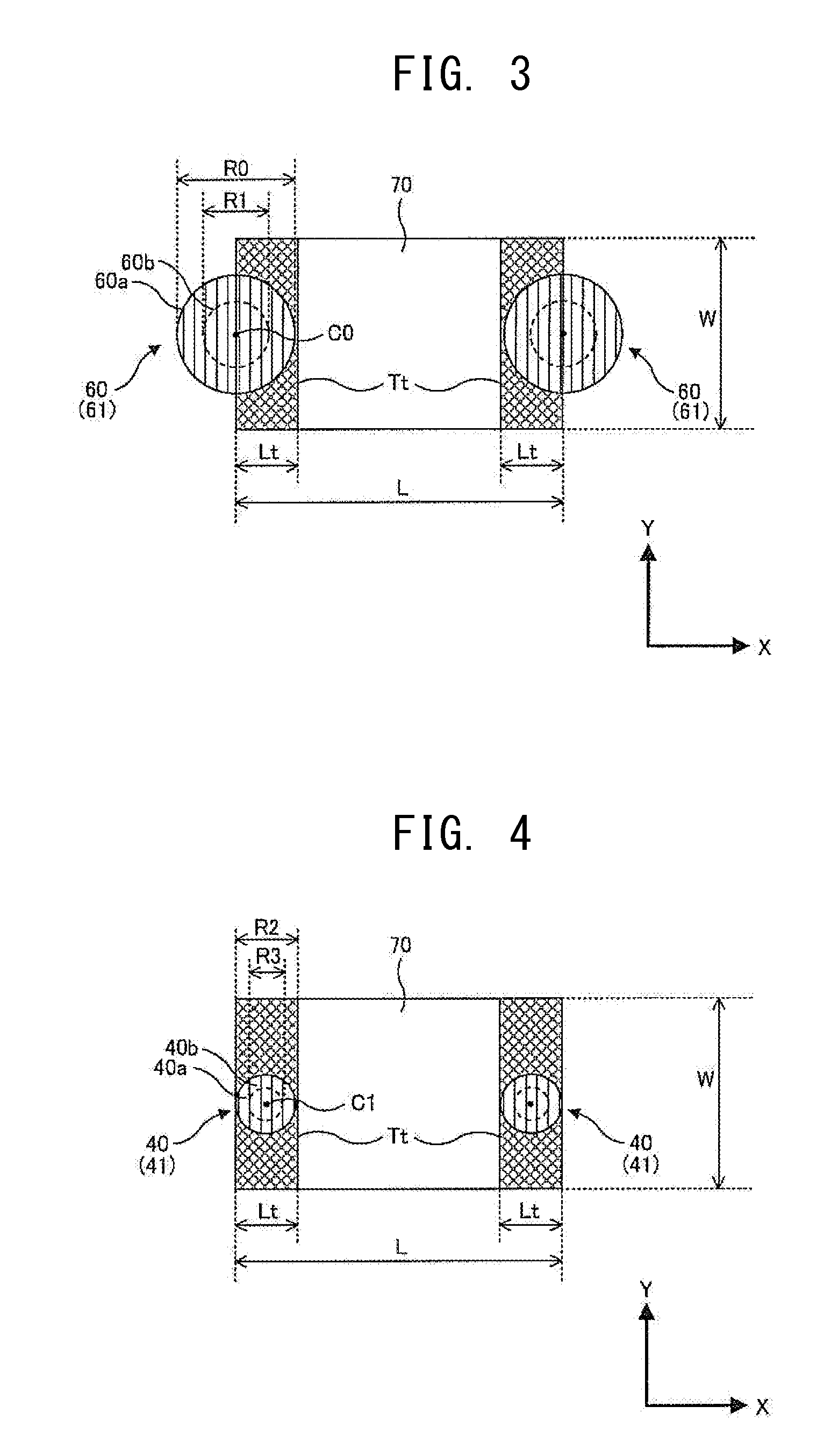
[0033]First, the structure of a component-incorporated wiring substrate according to an embodiment of the present invention will be described. FIG. 1 is a schematic sectional view showing the structure of a wiring substrate 10 having a built-in component (hereinafter referred to as “the wiring substrate 10”) of the present embodiment. As shown in FIG. 1, the wiring substrate 10 of the present embodiment includes a core substrate 11 formed from, for example, an epoxy resin which contains glass fiber, a build-up layer 12 on a side toward the upper surface of the core substrate 11, and a build-up layer 13 on a side toward the lower surface of the core substrate 11. The...


PUM

PropertyMeasurementUnit
diameteraaaaaaaaaa
lengthaaaaaaaaaa
via diameteraaaaaaaaaa

Abstract

A component-incorporated wiring substrate is provided. Some embodiments include a plate-like component incorporated in a core substrate and a build-up layer having an insulation layer and a conductor layer disposed in alternating layers. The component has terminal electrodes formed at its opposite ends having a side surface and a main surface. An insulation layer disposed on the main surface of the component has via conductors formed therein which are connected to the side surfaces and the main surfaces of the respective terminal electrodes. The via conductors are tapered, such that their via diameter decreases in a direction toward the terminal electrode, and their via diameter at a position where they connect to the main surface is greater than a length of the main surface. Accordingly, the area of connection between the via conductors and the corresponding terminal electrodes is increased, improving connection reliability through enhancement of tolerance for positional deviation.

Description

CROSS REFERENCE TO RELATED APPLICATIONS[0001]The present application claims priority from Japanese Patent Application No. 2011-189169, which was filed on Aug. 31, 2011, the disclosure of which is herein incorporated by reference in its entirety.BACKGROUND OF THE INVENTION[0002]1. Field of the Invention[0003]The present invention relates to a wiring substrate having a built-in component (hereinafter referred to as a “component-incorporated wiring substrate”) in which a plate-like component is incorporated.[0004]2. Description of Related Art[0005]A known package is configured as follows: build-up layers are formed on respective opposite sides of a core substrate so as to configure a wiring substrate, and an IC chip or a like device is mounted on the wiring substrate. In recent years, in association with an increase in speed and the number of terminals of IC chips, supply of power to the IC chip mounted on the wiring substrate from an external board involves a problem of malfunction ca...

Claims


Application Information

Patent Timeline
Patent Type & Authority Patents(United States)
IPC IPC(8): H05K1/16H05K1/09H05K1/11H05K1/18H05K3/30H01L23/498H01L23/50H01L23/64H05K1/02H05K3/46
CPCH05K1/185H01L23/642H01L23/49822H05K3/4602H05K2201/0187H05K2201/09827H05K2201/09854H05K2201/10015H05K2201/10636H05K2201/10734H05K1/0231H05K2203/1469H01L2224/16225H01L2924/15311H01L23/49827H01L23/50Y02P70/50Y10T29/49139
Inventor YAMASHITA, DAISUKEHIGO, KAZUNAGATSUKADA, TETSUJI
Owner NGK SPARK PLUG CO LTD
Why Eureka
Try Eureka