Method for driving light-emitting device

a technology of light-emitting devices and light-emitting elements, which is applied in the direction of static indicating devices, identification means, instruments, etc., can solve the problems of reducing the luminance of light-emitting elements, affecting the operation of light-emitting devices, so as to reduce the size and weight of light-emitting devices, and double the area displaying images

Inactive Publication Date: 2015-02-17
SEMICON ENERGY LAB CO LTD
View PDF40 Cites 6 Cited by
  • Summary
  • Abstract
  • Description
  • Claims
  • Application Information

AI Technical Summary

Benefits of technology

The invention provides a light emitting device that can suppress variations in brightness caused by variations in TFTs, changes in gate voltage, and deterioration of the electro luminescent material. It also allows for switching between image directions without adding a frame memory. This device has multiple functions and reduces size and weight of electronic apparatuses.

Problems solved by technology

TFTs using polycrystalline silicon have a problem that there are variations in characteristics due to a defect generated in a crystal grain boundary.
Further, there is another problem that the luminance of a light emitting element is lowered as an electro luminescent material deteriorates.
Deterioration of an electro luminescent material causes drop in luminance, even when a constant current is supplied to a light emitting element.
Therefore, when the level of gray scale changes per pixel in accordance with an image to be displayed, the level of deterioration of a light emitting element varies in each pixel, leading to variations in luminance.
However, it takes time and cost to optimize the process of transistor so as to realize both the low off-current of the transistor for controlling a video signal input to a pixel and the high on-current thereof to increase the capacitance.
Further, the gate voltage Vgs of the transistor for controlling a current supplied to a light emitting element is sensitive to switching of other transistors, variations in potentials of a signal line and a scan line and the like due to parasitic capacitance of the gate.
Although a light emitting device contributes to multiple functions of a portable electronic apparatus and reduction in the size and weight thereof, it has a difficulty in increasing the size of display screen.

Method used


Image

  • Method for driving light-emitting device
  • Method for driving light-emitting device
  • Method for driving light-emitting device

Examples


embodiment mode 1

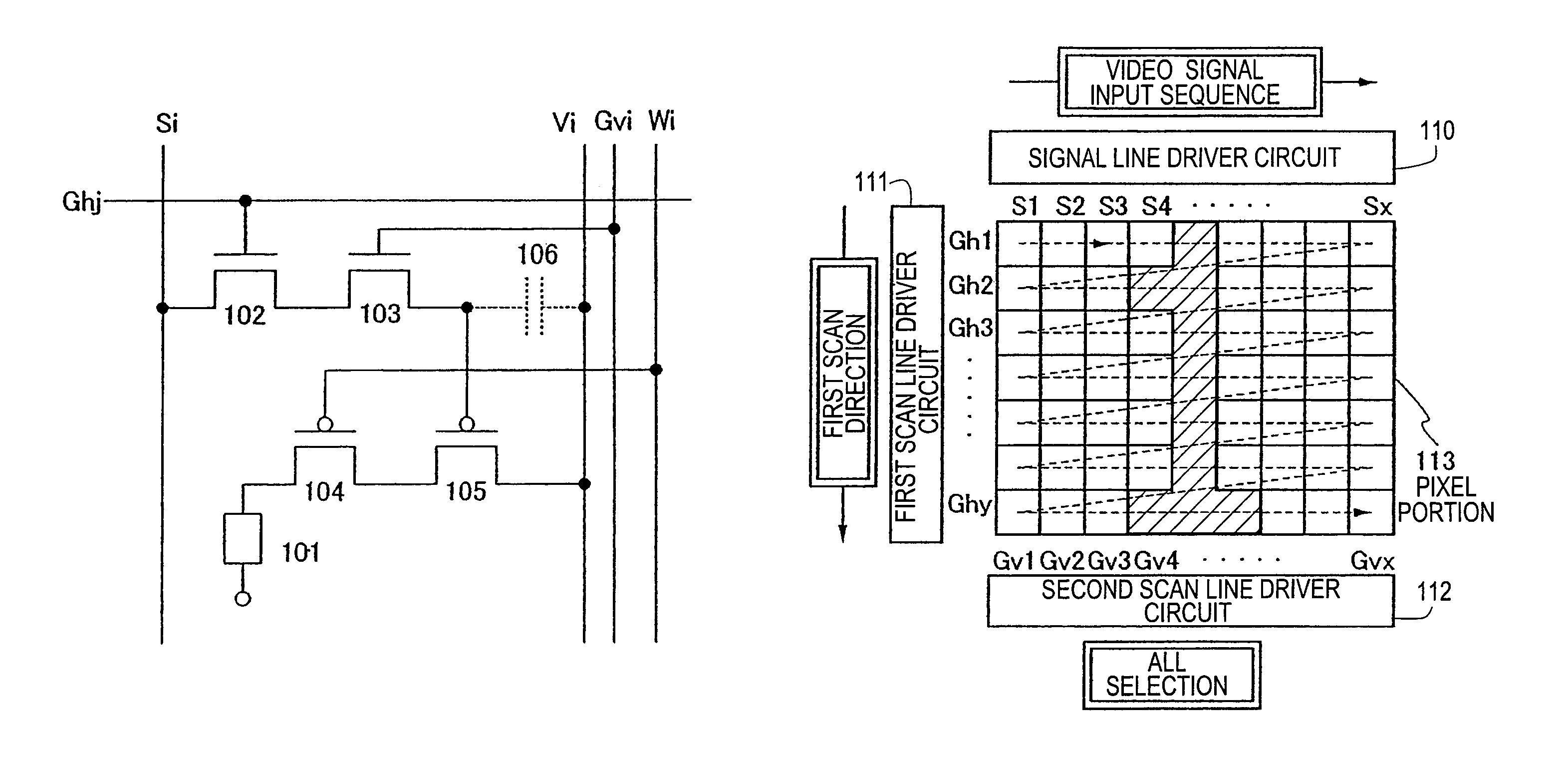
[0040]First, a configuration of a pixel included in the light emitting device of the invention will be described with reference to FIG. 1.

[0041]FIG. 1 shows an example of a pixel included in the light emitting device of the invention. The pixel shown in FIG. 1 comprises a light emitting element 101, two transistors (a first switching transistor 102 and a second switching transistor 103) used as switching elements for controlling a video signal input to the pixel, a driving transistor 104 for controlling a current value supplied to the light emitting element 101, and a current controlling transistor 105 for selecting whether a current is supplied to the light emitting element 101 or not. The pixel may also comprise a capacitor 106 for holding a video signal potential as shown in this embodiment mode.

[0042]The first switching transistor 102 and the second switching transistor 103 may have either the same conductivity or different conductivities. Although both the two switching transis...

embodiment mode 2

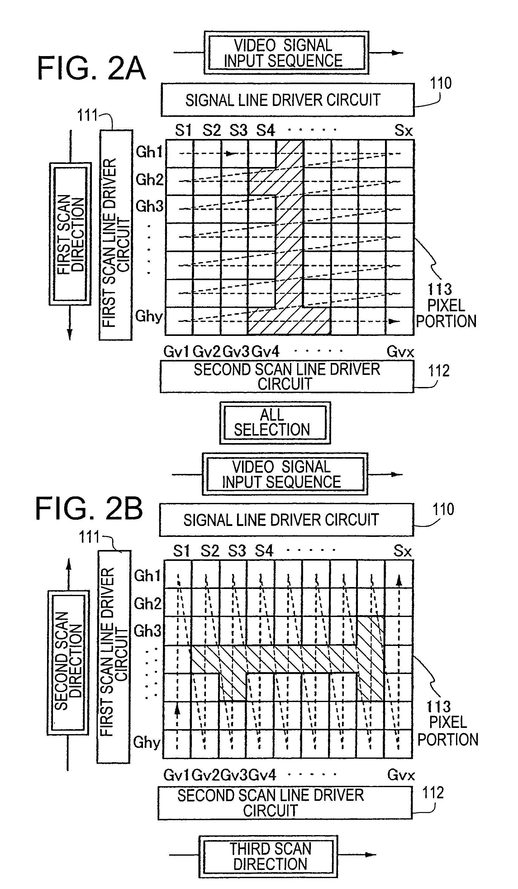
[0070]Explained in this embodiment mode is a structure of the light emitting device of the invention in which light is emitted from each side of a light emitting element.

[0071]In the case of a dual emission display device, an image is inverted to be displayed on each screen. Therefore, when switching a display screen, it is necessary to change an input sequence of a video signal from a signal line driver circuit to a signal line and a scan direction of a second scan line driver circuit as well as to change an image direction vertically to horizontally.

[0072]First, an operation for inverting the image shown in FIG. 2A left to right is explained with reference to FIG. 3A. In this case, the second scan lines Gv1 to Gvx are selected all at once as in FIG. 2A and the first scan lines Gh1 to Ghy are scanned in the same sequence as in FIG. 2A. In FIG. 3A, however, a video signal input from the signal line driver circuit 110 to the signal lines S1 to Sx is performed in the reverse order fro...

embodiment mode 3

[0080]Described in this embodiment mode is a configuration of the pixel shown in FIG. 1, which is added with a function for stopping light emission of a light emitting element independently on a video signal.

[0081]FIG. 5 shows an example of a pixel included in the light emitting device of the invention. The pixel shown in FIG. 5 comprises a light emitting element 401, two switching transistors 402 and 403 used as switching elements controlling a video signal input to the pixel, a driving transistor 404 for controlling a current value supplied to the light emitting element 401, a current controlling transistor 405 for selecting whether a current is supplied to the light emitting element 401 or not, and two erasing transistors 407 and 408 for stopping light emission of the light emitting element 401. The pixel may also comprise a capacitor 406 for holding a video signal potential as shown in this embodiment mode.

[0082]As in the pixel shown in FIG. 1, the first switching transistor 402...


PUM

PropertyMeasurementUnit
temperatureaaaaaaaaaa
radius of curvatureaaaaaaaaaa
sizeaaaaaaaaaa

Abstract

A light emitting device capable of suppressing drop in luminance or luminance unevenness of a light emitting element due to deterioration of an electro luminescent material and capable of switching an image direction vertically to horizontally without a frame memory additionally provided. The light emitting device of the invention comprises in each pixel first to fourth transistors, a light emitting element, and a signal line. The first transistor and the second transistor control the connection between the signal line and a gate of the third transistor, the fourth transistor controls a current value supplied to the light emitting element, and the third transistor selects whether the current is supplied to the light emitting element or not. Further, the first transistor and the second transistor are switched separately.

Description

BACKGROUND OF THE INVENTION[0001]1. Field of the Invention[0002]The present invention relates to a light emitting device capable of switching an image direction vertically to horizontally and also relates to an electronic apparatus using the light emitting device.[0003]2. Description of the Related Art[0004]A portable electronic apparatus typified by a mobile phone, an electronic notebook and the like requires multiple functions such as sending and receiving e-mail, voice recognition, taking-in images by a small camera as well as a display device for displaying images. On the other hand, reduction in the size and weight of the portable electronic apparatus is still sought for satisfying the user needs. Therefore, as many ICs having larger circuit scale and memory capacity as possible are required to be mounted on the narrow space of the portable electronic apparatus. It is an essential part to make a flat panel display to be mounted as thin and light as possible in order to achieve ...

Claims


Application Information

Patent Timeline
Patent Type & Authority Patents(United States)
IPC IPC(8): G09G3/30H01L51/50G02F1/1343G09F9/30G09G3/20G09G3/32H01L27/32H05B33/14
CPCG09G3/3233G09G3/3266G09G3/3291G09G2300/0426G09G2300/0814G09G2300/0842G09G2300/0861G09G2300/0866G09G2310/0251G09G2320/0223G09G2320/0233G09G2340/0492
Inventor KOYAMA, JUNOSAME, MITSUAKIYAMAZAKI, YUANZAI, AYA
Owner SEMICON ENERGY LAB CO LTD
Why Eureka
Try Eureka