
Frequency compensation techniques for low-power and small-area multistage amplifiers

a multi-stage amplifier, low-power technology, applied in the field of amplifiers, can solve the problems of high-frequency gain droop, low-power and small-area settling time, etc., and achieve the effect of expanding the drivability of the present invention with small power and area

Active Publication Date: 2015-02-24
UNIVERSITY OF MACAU
View PDF2 Cites 4 Cited by
  • Summary
  • Abstract
  • Description
  • Claims
  • Application Information

AI Technical Summary

Benefits of technology

The present invention is a three-stage amplifier that is designed to be powerful and efficient with small power and area. It includes a frequency compensation circuit and an active left-half plane zero circuit that work together to extend its usage with minimal effort.

Problems solved by technology

This regrettably penalizes the cost, settling time and high-frequency gain droop.

Method used


Image

  • Frequency compensation techniques for low-power and small-area multistage amplifiers
  • Frequency compensation techniques for low-power and small-area multistage amplifiers
  • Frequency compensation techniques for low-power and small-area multistage amplifiers

Examples


Embodiment Construction

[0028]Various exemplary embodiments, features, and aspects of the invention will be described in detail below with reference to the drawings. For the drawings below, the same or the similar numbers and symbols are referred to the same or the similar elements.

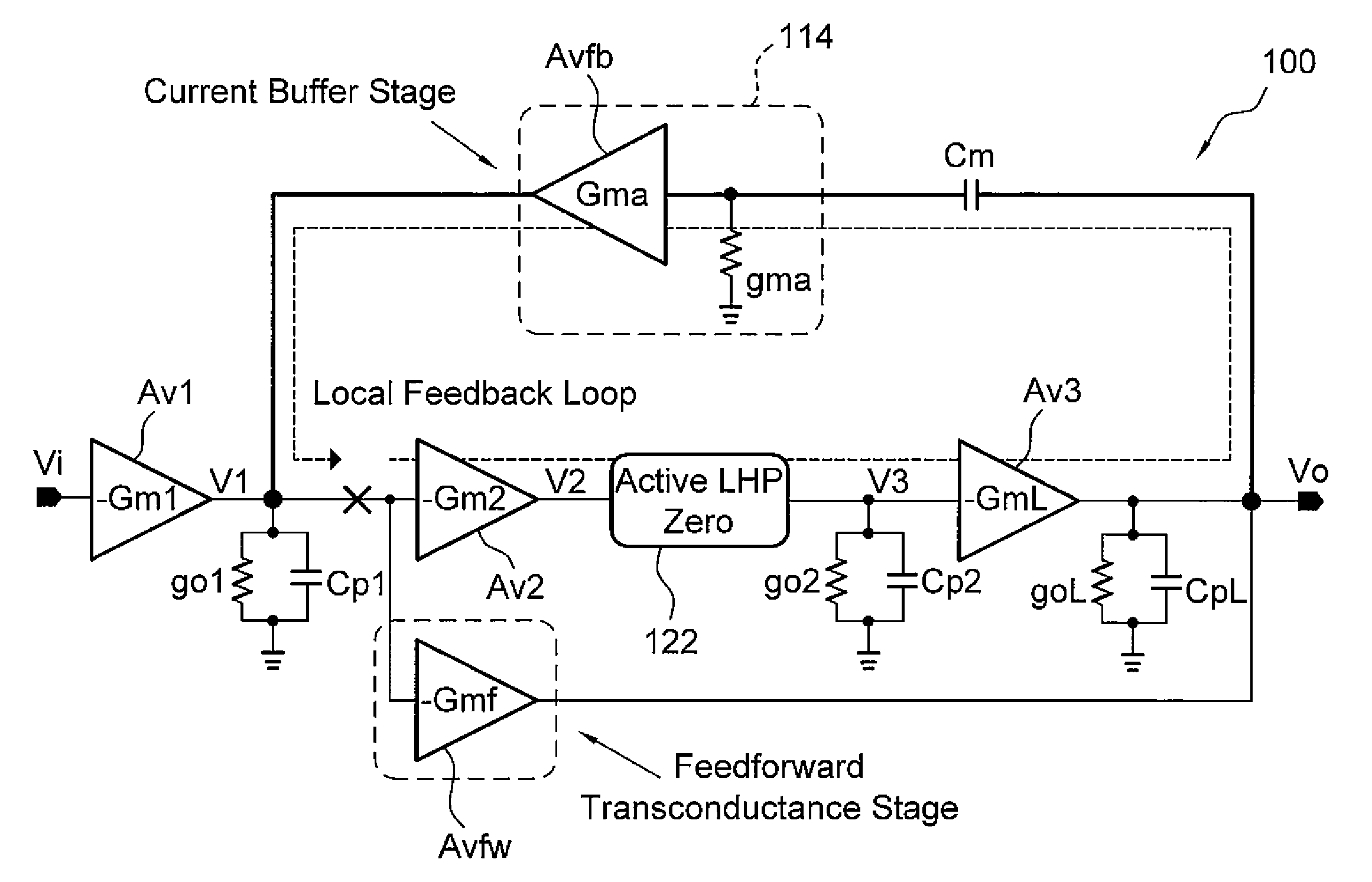
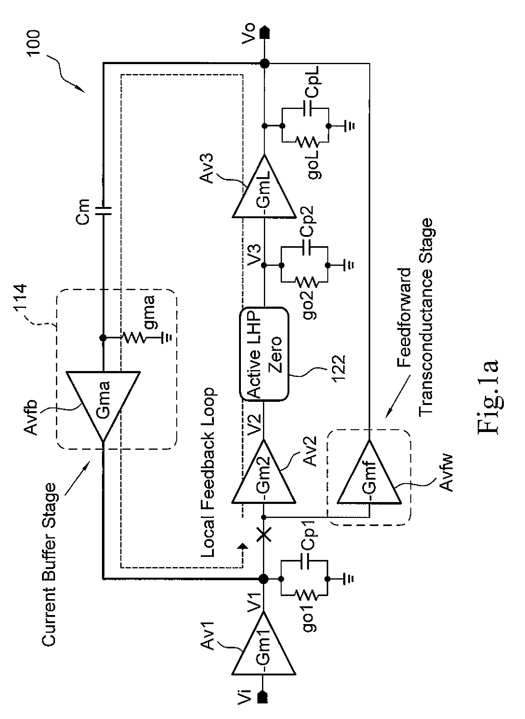
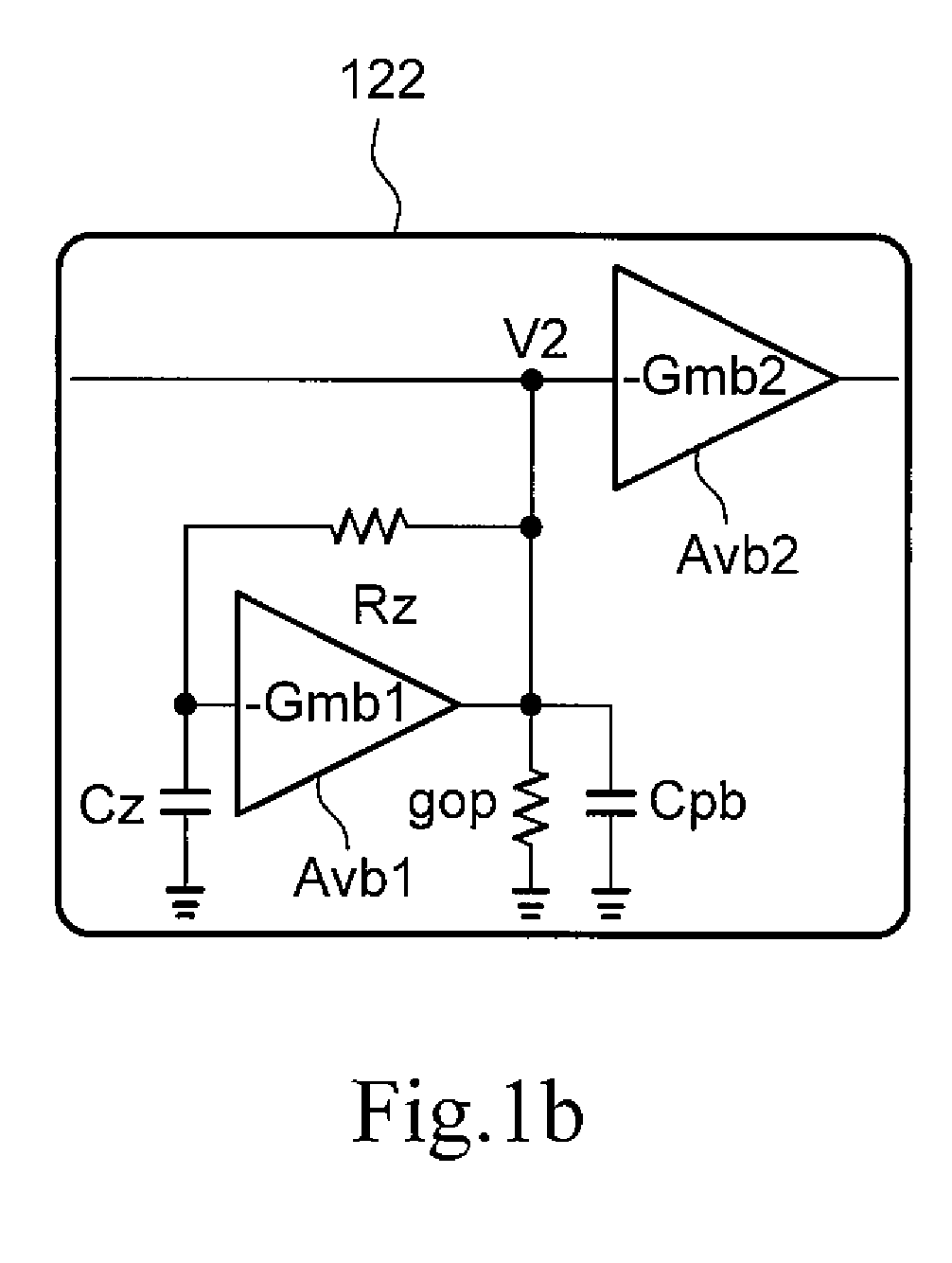
[0029]FIG. 1a shows a schematic circuit diagram illustrating the structure of a three stage amplifier 100 according to an embodiment of the invention. Referring to FIG. 1a, the three stage amplifier 100 comprises three main gain stages Av1, Av2, and Av3. In addition to the three main gain stages, the three stage amplifier 100 further comprises a feedforward transconductance stage Avfw, an active left half plane zero stage 122, a current buffer stage 114 and a Miller compensation capacitance Cm. Besides, there exists parasitic capacitances Cp1, Cp2, and parasitic transconductance resistances go1, go2, goL.

[0030]The gain stage Av1 receives an amplifier input signal Vi and generates a signal V1 depending on a negative transconducta...


PUM


Abstract

A three stage amplifier is provided and the three stage amplifier comprises a first gain stage, a second gain stage and a third gain stage wherein said first stage receives an amplifier input signal and said third gain stage outputs an amplifier output signal. The amplifier includes a feedback loop having a current buffer and a compensation capacitance provided from the output of said third gain stage to the output of the first gain stage. In addition, an active left half plane zero stage is embedded in said feedback loop for cancelling a parasitic pole of said feedback loop.

Description

BACKGROUND OF THE INVENTION[0001]1. Field of the Invention[0002]The present invention is related to an amplifier, and, in particular, to an amplifier with small power and area.[0003]2. Description of the Related Art[0004]High-color-depth LCD drivers demand an extensive number of amplifiers to buffer the Gamma-corrected reference voltages, which have to be stabilized by nF-range capacitors to handle the glitch energy during the digital-to-analog conversion. To deal with such a large capacitive load (CL), most commercial buffer amplifiers require an external resistor (e.g., 20Ω for CL=10 nF) in series with the output for ringing reduction. This regrettably penalizes the cost, settling time and high-frequency gain droop.SUMMARY OF THE INVENTION[0005]The present invention is directed to a three stage amplifier. The three stage amplifier includes first, second and third gain stages wherein said first stage receives an amplifier input signal and said third gain stage outputs an amplifier ...

Claims


Application Information

Patent Timeline
Patent Type & Authority Patents(United States)
IPC IPC(8): H03F3/45
CPCH03F3/45192H03F2200/408H03F2203/45631H03F2203/45674
Inventor YAN, ZUSHUMAK, PUI-INLAW, MAN-KAYMARTINS, RUI PAULO DA SILVA
Owner UNIVERSITY OF MACAU
Learn More