Quantum electro-optical device using CMOS transistor with reverse polarity drain implant

a reverse polarity drain and electro-optical device technology, applied in the field of integrated circuits (ics), can solve problems such as the problem of integrating quantum well electro-optical devices in silicon ics with energy level separations greater than 50 mev to allow operation at room temperatur

Active Publication Date: 2015-04-07
TEXAS INSTR INC
View PDF2 Cites 10 Cited by
  • Summary
  • Abstract
  • Description
  • Claims
  • Application Information

AI Technical Summary

Benefits of technology

[0023]In accordance with an embodiment of the present invention, the method further comprises the step of biasing the type source region to a negative potential with respect to the substrate, so that a current through the source region to the drain region decreases when a magnitude of the negative potential is increased.

Problems solved by technology

Integrating quantum well electro-optical devices in silicon ICs which feature energy level separations greater than 50 meV to allow operation at room temperature has been problematic.

Method used


Image

  • Quantum electro-optical device using CMOS transistor with reverse polarity drain implant
  • Quantum electro-optical device using CMOS transistor with reverse polarity drain implant
  • Quantum electro-optical device using CMOS transistor with reverse polarity drain implant

Examples


Embodiment Construction

[0035]Refer now to the drawings wherein depicted elements are, for the sake of clarity, not necessarily shown to scale and wherein like or similar elements are designated by the same reference numeral through the several views.

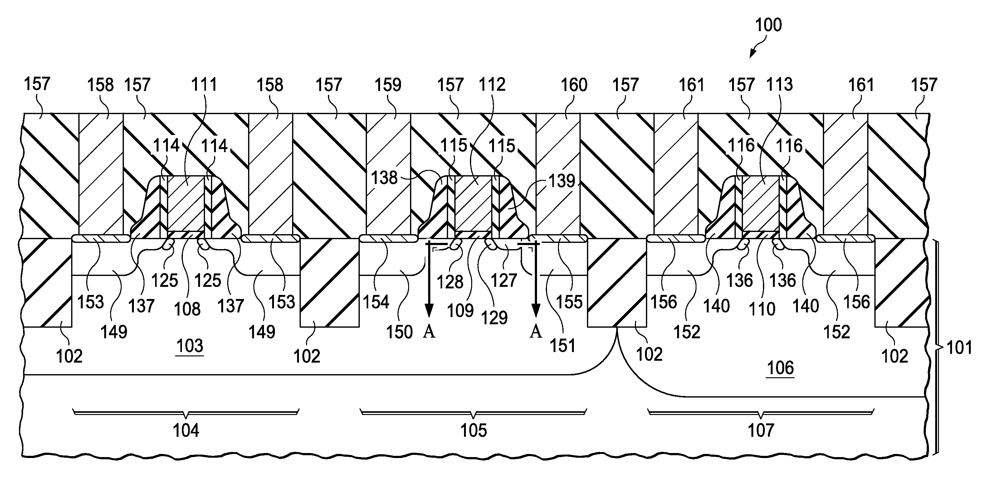
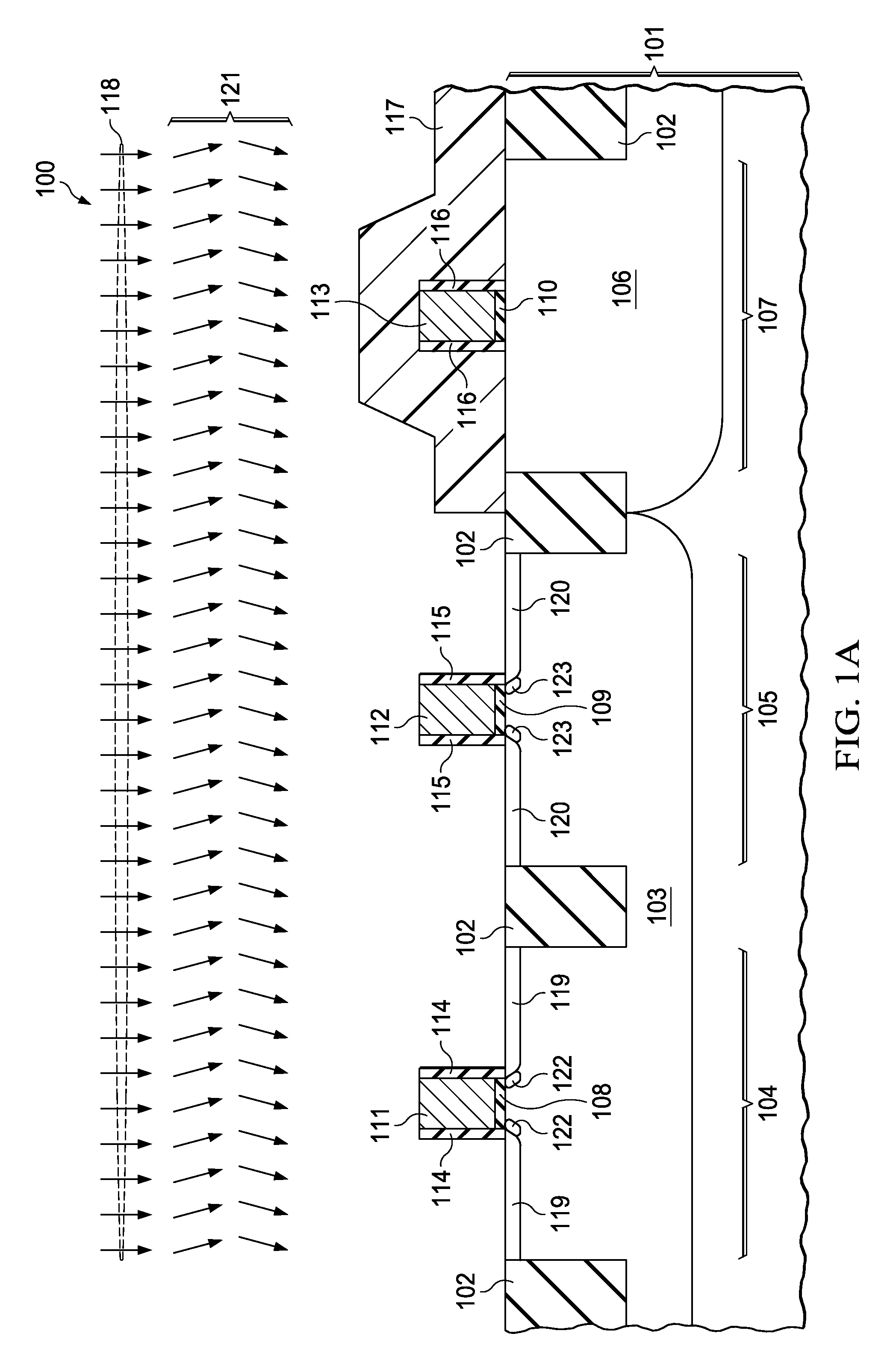
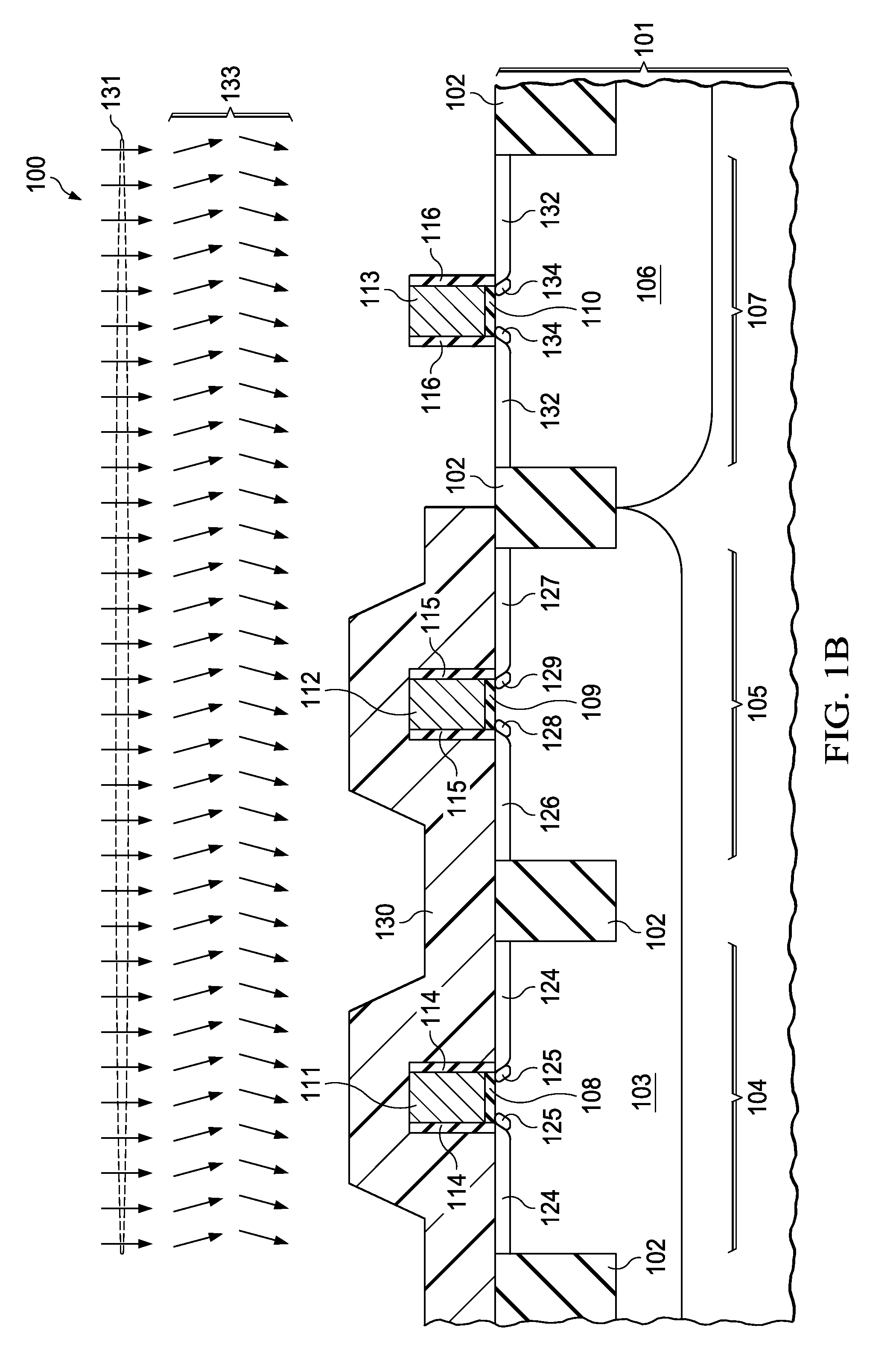
[0036]An IC is provided, containing a quantum well electro-optical device (QWEOD) which is formed in a modified NMOS transistor structure by ion implanting p-type dopants instead of n-type dopants into a drain region. A quantum well is formed in an n-type lightly doped drain (NLDD) region abutting the p-type drain region. Electrons may be transferred into, out of, and between discrete energy states in the quantum well by processes including tunneling to and from the p-type drain region, drifting through an n-type channel from an n-type source region, and photon absorption and emission. The QWEOD may be operated in a negative conductance mode, in a photon emission mode or in a photo detection mode. The QWEOD may be fabricated in a CMOS IC without adding process...


PUM


Abstract

A CMOS IC containing a quantum well electro-optical device (QWEOD) is disclosed. The QWEOD is formed in an NMOS transistor structure with a p-type drain region. The NLDD region abutting the p-type drain region forms a quantum well. The QWEOD may be fabricated with 65 nm technology node processes to have lateral dimensions less than 15 nm, enabling possible energy level separations above 50 meV. The quantum well electro-optical device may be operated in a negative conductance mode, in a photon emission mode or in a photo detection mode.

Description

CROSS-REFERENCE TO RELATED APPLICATIONS[0001]This application is a nonprovisional that claims priority from U.S. Provisional Application No. 61 / 405,085, filed Oct. 20, 2010, which is hereby incorporated by reference for all purposes.FIELD OF THE INVENTION[0002]This invention relates to the field of integrated circuits (ICs). More particularly, this invention relates to quantum electro-optical devices in ICs.BACKGROUND OF THE INVENTION[0003]Electro-optical devices based on quantum wells offer advantages over conventional electro-optical devices based on bulk semiconductor properties. Integrating quantum well electro-optical devices in silicon ICs which feature energy level separations greater than 50 meV to allow operation at room temperature has been problematic.SUMMARY OF THE INVENTION[0004]In accordance with an embodiment of the present invention, an integrated circuit (IC) is provided. The IC comprises a p-type substrate; a gate dielectric layer formed on a top surface of the sub...

Claims


Application Information

Patent Timeline
Patent Type & Authority Patents(United States)
IPC IPC(8): H01L21/336H01L21/8234H01L29/78H01L21/265H01L21/8238H01L29/10
CPCH01L21/823814H01L21/26586H01L29/1083H01L29/7833H01L29/122
Inventor EDWARDS, HENRY L.CHATTERJEE, TATHAGATABOWEN, ROBERT C.
Owner TEXAS INSTR INC
Why Eureka
Try Eureka