Semicondutor device package placed within fitting portion of wiring member and attached to heat sink

a semiconductor device and wiring member technology, applied in the direction of printed circuit aspects, printed circuit non-printed electric components association, basic electric elements, etc., can solve the problem of increasing the number of working steps, difficult to determine whether the protruding portion of the semiconductor device has been reliably inserted into the fitting hole, etc., to achieve the effect of reliably and easily putting the semiconductor devi

Active Publication Date: 2015-04-14
MITSUBISHI ELECTRIC CORP
View PDF13 Cites 1 Cited by
  • Summary
  • Abstract
  • Description
  • Claims
  • Application Information

AI Technical Summary

Benefits of technology

[0010]The invention was devised to solve the problems discussed above and is to provide a semiconductor apparatus configured to position a semiconductor device reliably and easily without having a protruding portion formed in the bottom surface of the semiconductor device in the semiconductor apparatus.
[0012]According to the semiconductor apparatus of the invention, it becomes possible to position the semiconductor device at a high degree of accuracy. Moreover, assembly performance is enhanced because assembling is carried out by confirming the positioning portion. It thus becomes possible to obtain a semiconductor apparatus capable of reducing the occurrence of deficient mounting of the semiconductor device.

Problems solved by technology

This configuration, however, makes it difficult to provide the protruding portion for a semiconductor device having an electrode or a heat spreader that spreads out heat generated at the semiconductor device on the bottom surface thereof.
Also, because it is necessary to drill the fitting hole in the printed circuit board or the heat sink on which the semiconductor device is mounted, there is a problem that the number of working steps is increased.
Further, in the step of attaching the semiconductor device, there is another problem that it is difficult to determine whether the protruding portion of the semiconductor device has been inserted reliably into the fitting hole when viewed from the top surface of the semiconductor device.
This configuration raises a problem that high-accurate positioning is difficult to achieve.

Method used


Image

  • Semicondutor device package placed within fitting portion of wiring member and attached to heat sink
  • Semicondutor device package placed within fitting portion of wiring member and attached to heat sink
  • Semicondutor device package placed within fitting portion of wiring member and attached to heat sink

Examples


first embodiment

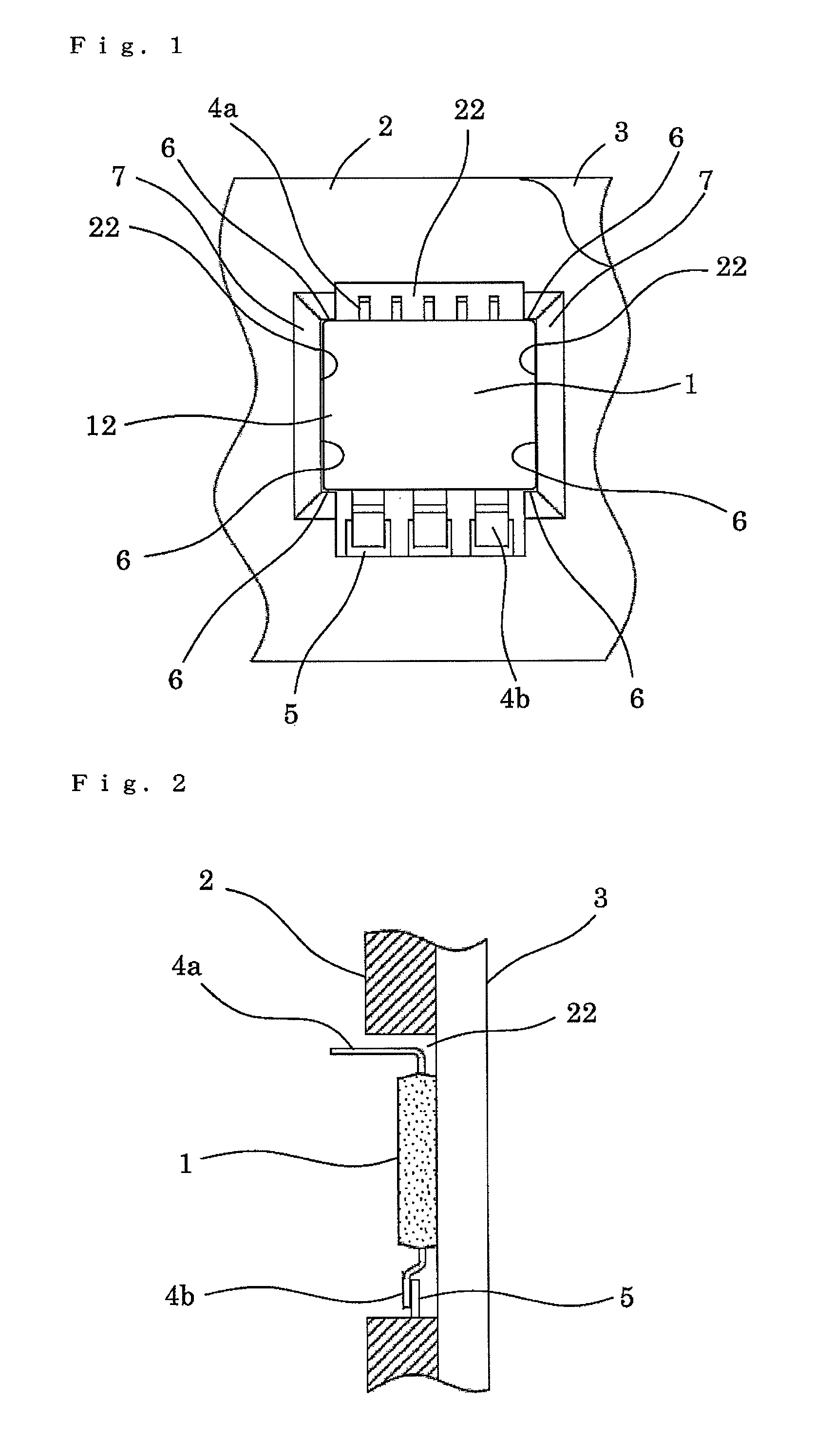
[0021]Hereinafter, a first embodiment of the invention will be described on the basis of FIG. 1 through FIG. 3, and descriptions will be given by labeling same or equivalent members and portions with same reference numerals in the respective drawings. FIG. 1 is a plan view of a semiconductor apparatus according to a first embodiment of the invention. FIG. 2 is a longitudinal cross section of the semiconductor apparatus according to the first embodiment of the invention. FIG. 3 is a transverse cross section of the semiconductor apparatus according to the first embodiment of the invention.

[0022]Referring to FIG. 1 through FIG. 3, the semiconductor apparatus according to the first embodiment of the invention includes a semiconductor device 1, a wiring member 2, and a heat sink 3. The semiconductor device 1 in the semiconductor apparatus is of a surface mount package type and it has a flat package main body 12 made of resin. Although it is not shown in the drawings, a semiconductor devi...

second embodiment

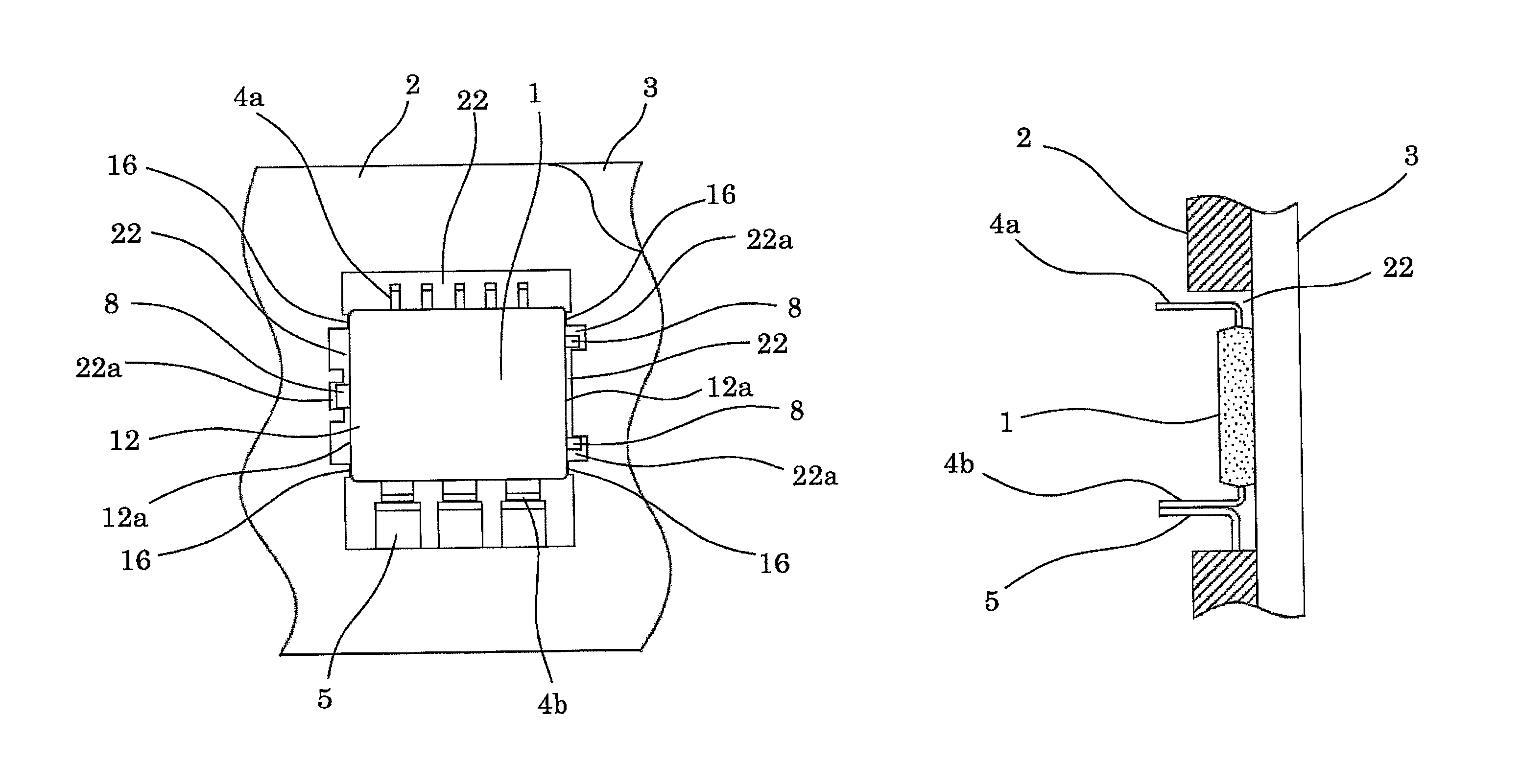
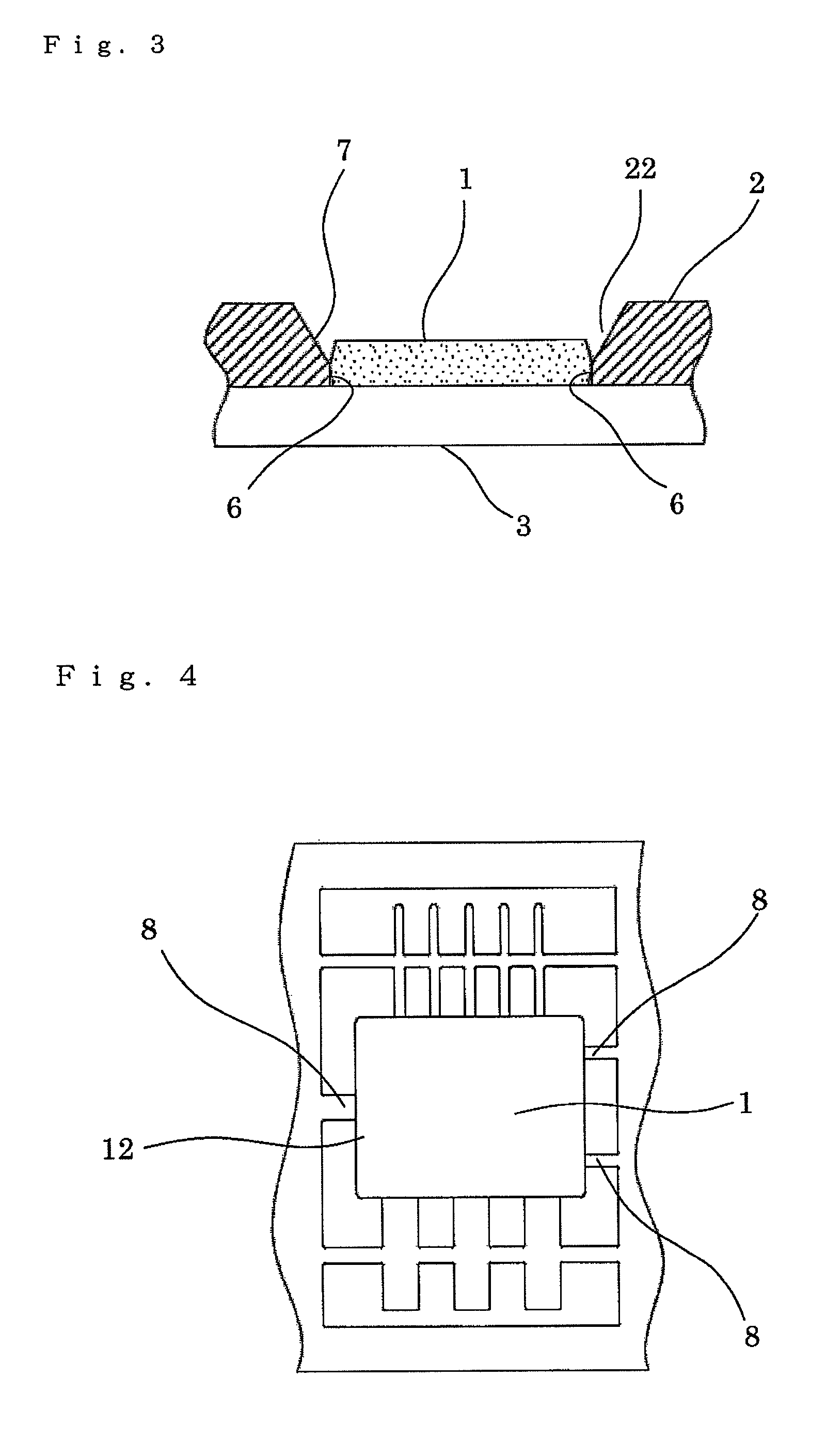
[0030]A second embodiment of the invention will be described on the basis of FIG. 4 through FIG. 6, and descriptions will be given by labeling same or equivalent members and portions with same reference numerals in the respective drawings. FIG. 4 is a plan view of a semiconductor device in a semiconductor apparatus according to the second embodiment of the invention. FIG. 5 is a plan view of the semiconductor apparatus according to the second embodiment of the invention. FIG. 6 is a longitudinal cross section of the semiconductor apparatus according to the second embodiment of the invention.

[0031]Referring to FIG. 4 through FIG. 6, a semiconductor device 1 in the semiconductor apparatus is of a surface mount package type and has a flat package main body 12 made of resin. Although it is not shown in the drawings, a semiconductor chip is attached inside the package main body 12 and a large number of leads made of a metal material and electrically connected to the semiconductor chip ar...


PUM


Abstract

The invention is to provide a semiconductor apparatus configured to position a semiconductor device reliably and easily without having a protruding portion formed in the bottom surface of the semiconductor device in the semiconductor apparatus. A semiconductor apparatus is fabricated by attaching a semiconductor device of a surface mount package type and a wiring member to a heat sink. A fitting portion in which the semiconductor device is fit is provided to the wiring member, so that the semiconductor device is positioned by fitting the semiconductor device into the fitting portion provided to the wiring member. According to the semiconductor apparatus of the invention, it becomes possible to position the semiconductor device at a high degree of accuracy.

Description

BACKGROUND OF THE INVENTION[0001]1. Field of the Invention[0002]The present invention relates to a semiconductor apparatus including, for example, a semiconductor device of a surface mount package type.[0003]2. Description of the Related Art[0004]In a semiconductor apparatus in the related art, a protruding portion is provided to the bottom surface of a semiconductor device of a surface mount package type (hereinafter, referred to as the semiconductor device) and a fitting hole in which the protruding portion is fit is made in a printed circuit board or a heat sink on which the semiconductor device is mounted. This semiconductor apparatus is structured in such a manner that the semiconductor device is attached and positioned by fitting the protruding portion of the semiconductor device into the fitting hole made in the printed circuit board or the heat sink on the mounting side. Examples are disclosed in JP-A-6-268086 and JP-T-2008-543266 (Japanese Patent Application No. 2008-514162...

Claims


Application Information

Patent Timeline
Patent Type & Authority Patents(United States)
IPC IPC(8): H01L23/40H01L23/36H05K1/02H05K1/18
CPCH05K1/021H01L23/4093H01L23/36H05K1/184H05K2201/0397H05K2201/09118H05K2201/09827H05K2201/10166H05K2201/10689H01L2924/0002H01L2924/00H01L23/13
Inventor KATO, MASAKIFUJITA, MASAHIKOSAKAMOTO, KAZUYASU
Owner MITSUBISHI ELECTRIC CORP
Why Eureka
Try Eureka