
Automation for monolithic 3D devices

a technology of monolithic 3d devices and automatic design, applied in computing, instruments, electric digital data processing, etc., can solve the problems of large and elaborate cad tools, tens and hundreds of millions of modern designs, and achieve the effect of increasing the physical proximity of objects

Active Publication Date: 2015-04-28
MONOLITHIC 3D
View PDF10 Cites 35 Cited by
  • Summary
  • Abstract
  • Description
  • Claims
  • Application Information

AI Technical Summary

Benefits of technology

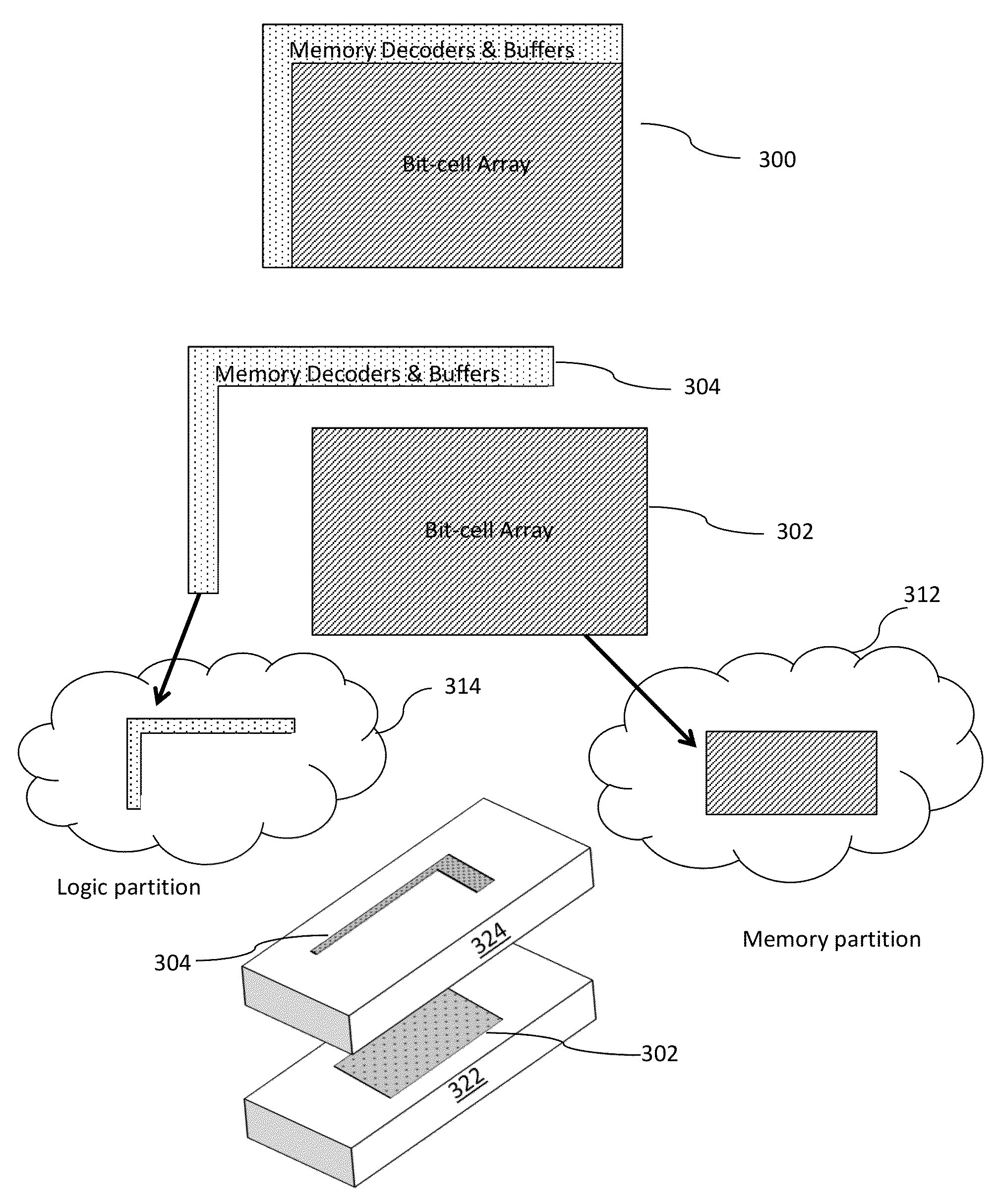
The invention provides increased functionality for CAD tools used in a monolithic 3D manufacturing process. The size of inter-layer connections in monolithic 3D technology is much smaller than in a stacked-layer process, so CAD tools should focus on leveraging the large inter-layer connectivity to optimally place objects on different layers based on their characteristics. The invention provides methods for designing 3D integrated circuits using a 2D placer, followed by placement for at least two strata, and then routing and completing the physical design. The design process takes advantage of the large inter-layer connectivity in monolithic 3D technology to optimize the placement of objects and improve the physical proximity of objects in 3D space.

Problems solved by technology

Modern designs routinely exceed tens and hundreds of millions of transistors and require massive and elaborate CAD tools to handle them.

Method used


Image

  • Automation for monolithic 3D devices
  • Automation for monolithic 3D devices
  • Automation for monolithic 3D devices

Examples


Embodiment Construction

[0020]Embodiments of the present invention are described herein with reference to the drawing figures. Persons of ordinary skill in the art will appreciate that the description and figures illustrate rather than limit the invention and that in general the figures are not drawn to scale for clarity of presentation. Such skilled persons will also realize that many more embodiments are possible by applying the inventive principles contained herein and that such embodiments fall within the scope of the invention which is not to be limited except by the appended claims.

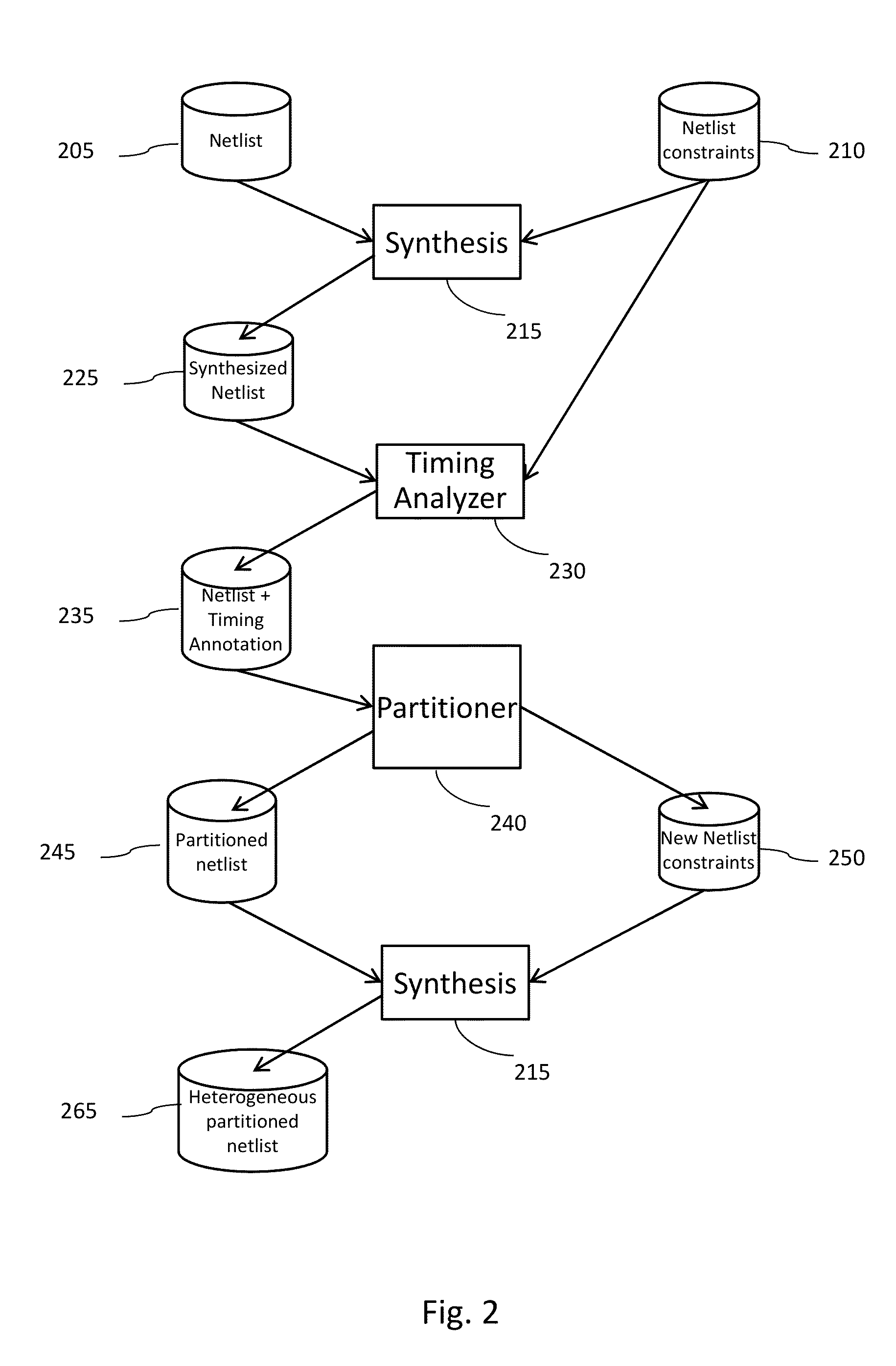
[0021]There are multiple known ways to partition a design, but the essential approach described in Metis (Karypis, G., Kumar, V., “METIS—Unstructured Graph Partitioning and Sparse Matrix Ordering,” 1995) subsumes most of them in modern CAD tools. It may consist of three phases: graph coarsening through clustering, followed by partitioning of the smaller resulting graph, followed by an uncoarsening phase. Most partitioners ...


PUM


Abstract

A method of designing a 3D Integrated Circuit, the method including: performing placement using a 2D placer, performing placement for at least a first strata and a second strata, and then performing routing and completing the physical design of said 3D Integrated Circuit.

Description

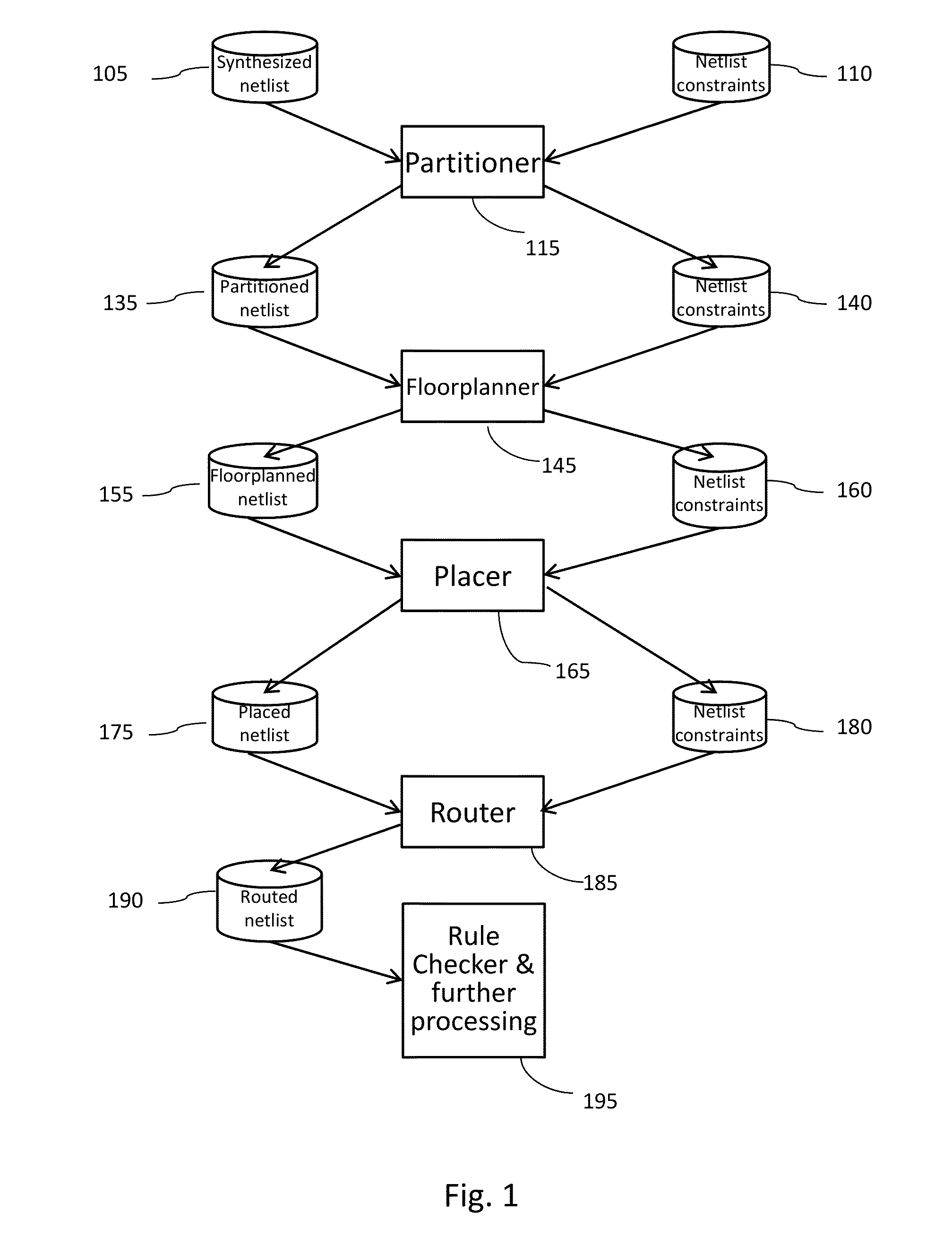
BACKGROUND OF THE INVENTION[0001]1. Field of the Invention[0002]This application relates to the general field of computer aided design of monolithic three-dimensional integrated circuits.[0003]2. Discussion of Background Art[0004]Use of computer programs for automating the design of electronic circuits, and particularly for assisting in the design of semiconductor integrated circuits, has been known for at least forty years. This field of Computer-Aided Design (CAD) encompasses the spectrum of engineering activities from early capture of the design idea, through its various refinements (both automatic and manual), modeling, simulations, down to its mapping to physical objects, partitioning and floor-planning, placement and routing, rule-checking and mask-making. The first part of these activities occurs in the logical domain, before mapping to physical objects (macros and cells) occurs, and is known as logic design. The part of the process after mapping the logical design to physica...

Claims


Application Information

Patent Timeline
IPC IPC(8): G06F17/50
CPCG06F17/5077G06F17/5072G06F30/394G06F30/392
Inventor OR-BACH, ZVIWURMAN, ZEEV
Owner MONOLITHIC 3D
Learn More