CMOS spacer structure and preparation method thereof

A side wall structure and isolation wall technology, which is applied in semiconductor/solid-state device manufacturing, electrical components, circuits, etc., can solve the problems of underlying silicon substrate damage, device performance degradation, damage, etc., to eliminate loss and increase physical distance , Improve the effect of filling conditions

Active Publication Date: 2013-12-04
SHANGHAI HUALI MICROELECTRONICS CORP
View PDF2 Cites 0 Cited by
  • Summary
  • Abstract
  • Description
  • Claims
  • Application Information

AI Technical Summary

Problems solved by technology

The above-mentioned process also adopts the gate without sidewall structure and the oxide layer-nitride layer (ON) structure. By increasing the width-to-depth ratio of the hole, it facilitates the filling of the pre-metal dielectric and reduces the probability of filling the void. However, when dry The underlying silicon substrate or silicide will be damaged when the sidewall is etched by method or wet method, and the offset spacer will be seriously damaged in the dry etching environment, resulting in gate damage and device failure. reduced performance of

Method used


Image

  • CMOS spacer structure and preparation method thereof
  • CMOS spacer structure and preparation method thereof
  • CMOS spacer structure and preparation method thereof

Examples


preparation example Construction

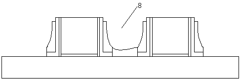
[0037] see Figure 3a As shown in -e, the present invention also provides a method for preparing a CMOS sidewall structure, the steps of which include:

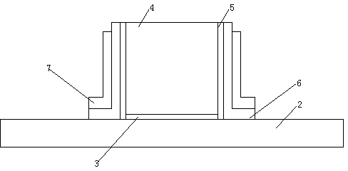
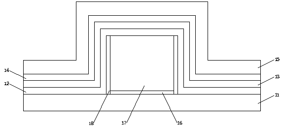
[0038] A first oxide layer 12, a first nitride layer 13, a second oxide layer 14 and a second nitride layer 15 are sequentially deposited on a silicon substrate 11 provided with a gate 17, wherein the side of the gate 17 A bias isolation wall 18 is arranged on the wall, and a dielectric layer 16 is arranged between the gate electrode 17 and the silicon substrate 11 .

[0039] Selective dry etching of the second nitride layer 15 to form a sidewall nitride layer 15 outside the second oxide layer 14 on the side of the gate 17 1 ; With the sidewall nitride layer 15 1 As a mask, wet etch the second oxide layer 14, etch away the second oxide layer at the top of the gate 17, and the sidewall nitride layer 15 1cover the other second oxide layer, and form an L-shaped outer oxide layer 14 outside the first nitride layer 13 on the si...


PUM


Abstract

The invention relates to the semiconductor integrated circuit manufacture field, concretely relating to a CMOS spacer structure and a preparation method thereof. The invention discloses the CMOS spacer structure and the preparation method thereof. Through employing an ONON structure and etching technology with combination of dry method etching and wet method etching, a spacer can be effectively removed, a physical distance of a bottom of a groove between adjacent grids is increased, filling condition of a pre-metal medium is improved, loss of a silicon substrate caused by dry method etching is effectively avoided, loss of silicide when using the wet method to remove the spacer is effectively avoided, and through reducing loss of an offset isolation wall in technology, the grids obtain full protection.

Description

technical field [0001] The present invention generally relates to the field of semiconductor integrated circuit manufacturing, more precisely, the present invention relates to a CMOS sidewall structure and a preparation method thereof. Background technique [0002] With the increasing integration of semiconductor components, heat dissipation and quantum tunneling have become new problems in chip miniaturization process technology, and strained silicon technology adopts a method that is relatively low in cost and can be applied on a large scale to increase the size of silicon atoms. The space between them can reduce the obstacles to the passage of electrons, that is, the resistance is reduced, the heat generation and energy consumption of the device are reduced to a certain extent, and the operating speed is improved, and this expanded space is the space for electrons to flow, thus effectively Reduced thermal issues and quantum tunneling. [0003] Currently, strained silicon...

Claims


Application Information

Patent Timeline
Patent Type & Authority Patents(China)
IPC IPC(8): H01L29/10H01L29/78H01L21/8238H01L21/336
Inventor 郑春生张文广徐强陈玉文
Owner SHANGHAI HUALI MICROELECTRONICS CORP
Why Eureka
Try Eureka