Power semiconductor device and manufacturing method

A technology for power semiconductors and manufacturing methods, applied in the fields of semiconductor/solid-state device manufacturing, semiconductor devices, semiconductor/solid-state device components, etc., can solve problems such as not being extended to high-voltage and high-power devices, and improve resistance to voltage breakdown. capacity, improved yield, and improved heat dissipation performance

Inactive Publication Date: 2022-04-29
晏新海
View PDF0 Cites 0 Cited by
  • Summary
  • Abstract
  • Description
  • Claims
  • Application Information

AI Technical Summary

Problems solved by technology

[0004] Although a small number of manufacturers recently launched bottom-source MOS products, that is to say, the source is connected to the base of the package, whether it is the traditional front-mount process, CLIP jumper package, or the newly developed bottom-source MOS products, technology, the bottom plate of the packaging frame has always been flat, and the bottom of the source has only introduced a small number of low-power, low-voltage, SMD packaged MOS products, which have not been extended to the high-voltage and high-power device category so far.

Method used


Image

  • Power semiconductor device and manufacturing method
  • Power semiconductor device and manufacturing method
  • Power semiconductor device and manufacturing method

Examples


Embodiment Construction

[0039] Hereinafter, the technical solution will be described in detail by taking a power MOS device as an example in combination with the accompanying drawings.

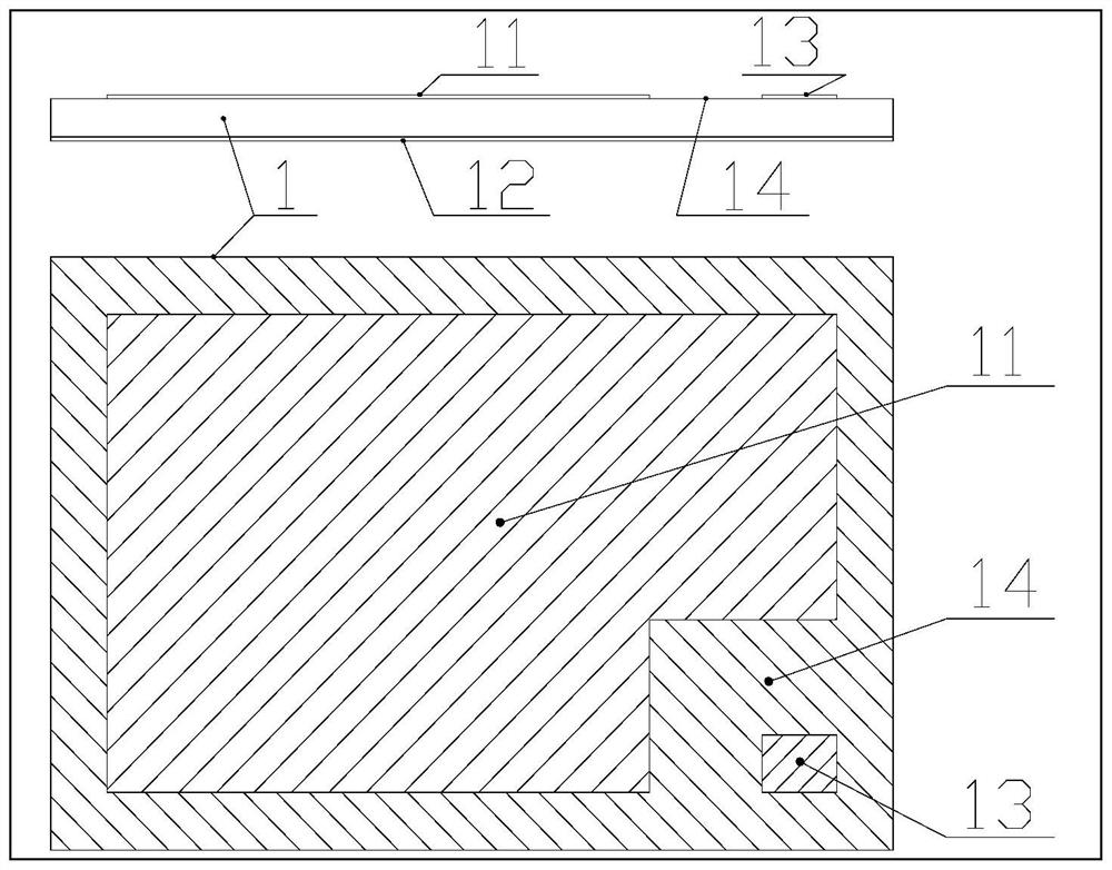
[0040] Power chip design and manufacture such as figure 1 , the power semiconductor device chip, according to the application parameter requirements of the power device, design and manufacture the power chip 1; Drain 12 on the back;

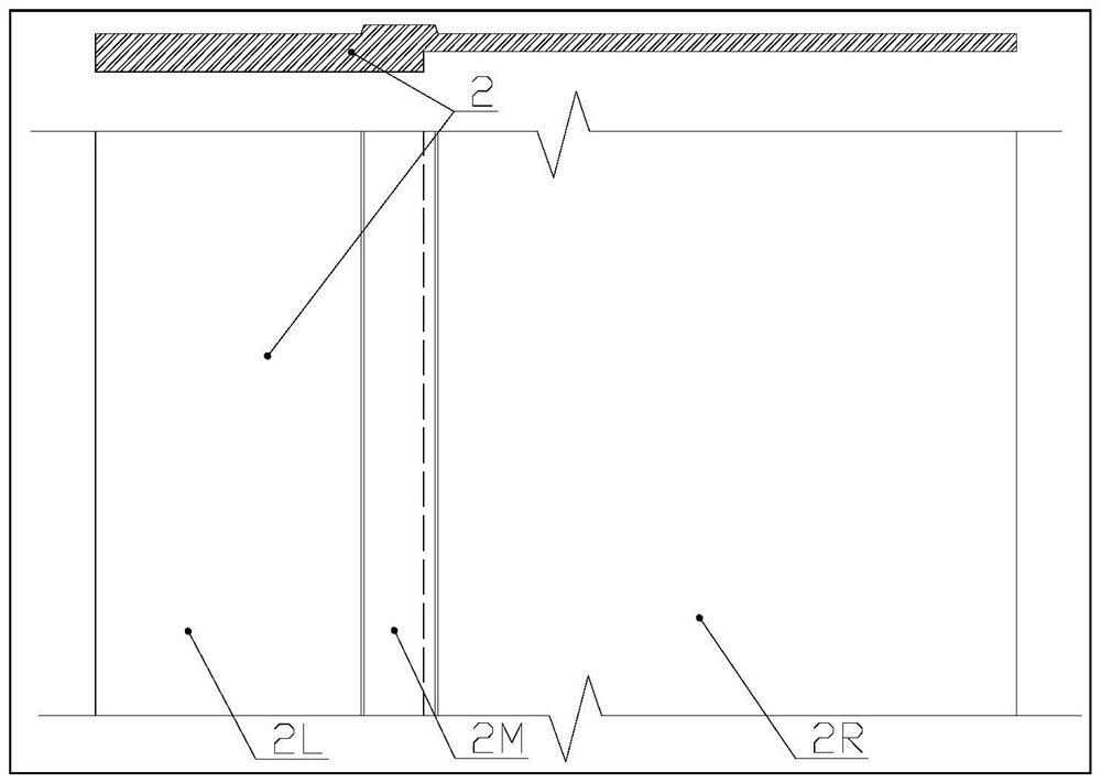
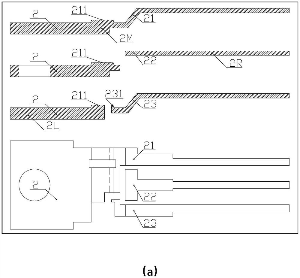
[0041] The source electrode 11 of the power chip is directly welded to the package frame 2, and is attached to the raised package copper frame and the chip source metal welding area 211. After welding, the source electrode connection is formed, and the heat generated by the chip 1 passes through the source electrode 11 and passes through the package frame. 2 Conduction to dissipate heat outward;

[0042] The drain 12 of the power chip is welded to the package frame 2 by wire bonding or CLIP jumper, and is connected to the drain pin 22 of the package copper frame;

[0043] The power ...


PUM


Abstract

The invention discloses a power semiconductor device and a manufacturing method thereof, a chip source electrode or an emitter electrode is directly welded to a packaging frame, and heat of a chip passes through the source electrode or the emitter electrode and is conducted outwards through a packaging frame base; and the welding areas of the frame and the source electrode or the emitter electrode and the grid electrode of the power chip are bulges. Protruding areas of the source electrode or the emitting electrode and the grid electrode of the frame are manufactured by punching and forming after the frame is extruded into strip-shaped copper strips, and the strip-shaped copper strips correspond to protrusions of areas where the source electrode or the emitting electrode and the grid electrode of the power chip are welded. The power semiconductor device and a common packaging power semiconductor device are consistent in appearance and pin arrangement, however, the thermal resistance is reduced by more than half, and the heat dissipation performance is obviously improved.

Description

technical field [0001] The invention belongs to the technical field of power semiconductor device manufacturing, and in particular relates to a device structure and a manufacturing method for improving the performance of a power semiconductor device. Background technique [0002] Power semiconductor devices such as MOS and IGBT currently produced usually have three electrodes, namely, the source or emitter electrode on the front, and the gate electrode, and the drain or collector electrode on the back. The history of the semiconductor industry has gradually developed from low frequency and low power, and gradually developed to high frequency and high power with the different needs of device applications. [0003] The design and manufacturing levels of early semiconductor devices were relatively low, so the production process was mainly to pursue simplicity and ease of operation. Obviously, one electrode is convenient for welding, and two electrodes are likely to cause electr...

Claims


Application Information

Patent Timeline
Patent Type & Authority Applications(China)
IPC IPC(8): H01L23/495H01L21/48H01L29/78
CPCH01L23/49568H01L23/4952H01L21/4825H01L29/78H01L2224/83385H01L2224/0603H01L2224/32245H01L2224/16245
Inventor 晏新海
Owner 晏新海
Why Eureka
Try Eureka