

Wafer packaging method
a packaging method and wafer technology, applied in the direction of electrical equipment, semiconductor devices, radio frequency controlled devices, etc., can solve the problems of difficulty in manufacturing process, more likely mechanical strength of thin glass, etc., and achieve the effect of easy alignment, increased strength of light transmissive protection sheets and wafers, and easy separation
- Summary
- Abstract
- Description
- Claims
- Application Information
AI Technical Summary
Benefits of technology
Problems solved by technology
Method used
Image

Examples
Embodiment Construction
[0048]Reference will now be made in detail to the present embodiments of the invention, examples of which are illustrated in the accompanying drawings. Wherever possible, the same reference numbers are used in the drawings and the description to refer to the same or like parts.
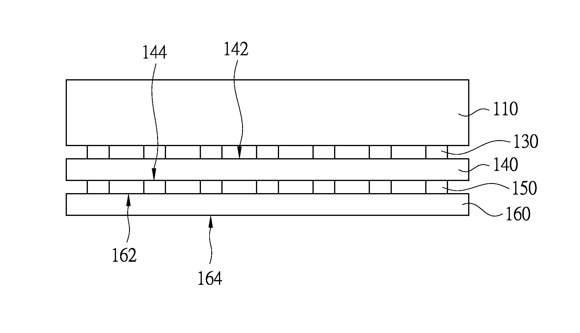
[0049]FIG. 3 is a flow chart of a wafer packaging method according to one embodiment of the present invention. In step S1, a light transmissive carrier is provided. Thereafter in step S2, a hydrolytic temporary bonding layer is formed on the light transmissive carrier. Next in step S3, a first surface of a light transmissive protection sheet is bonded to the hydrolytic temporary bonding layer, such that the hydrolytic temporary bonding layer is located between the light transmissive protection sheet and the light transmissive carrier. Thereafter in step S4, a second surface of the light transmissive protection sheet facing away from the first surface is bonded to a third surface of a wafer, and the third surfa...
PUM
 Abstract
Description
Claims
Application Information