Light emitting diode

a technology of light-emitting diodes and diodes, which is applied in the direction of material nanotechnology, solid-state devices, radiation control devices, etc., can solve the problems of uneven resistance over an entire area, poor mechanical durability of ito, and low chemical endurance,

Active Publication Date: 2015-05-26
BEIJING FUNATE INNOVATION TECH
View PDF8 Cites 0 Cited by
  • Summary
  • Abstract
  • Description
  • Claims
  • Application Information

AI Technical Summary

Benefits of technology

[0006]A standard light emitting diode (LED) includes an N-type semiconductor layer, a P-type semiconductor layer, an active layer located between the N-type semiconductor layer and the P-type semiconductor layer, a first electrode electrically connected to the N-type semiconductor layer, and a second electrode electrically connected to the P-type semiconductor layer. In an operation, a positive voltage and a negative voltage are applied respectively to the P-type semiconductor layer and the N-type semiconductor layer. Thus, holes in the P-type semiconductor layer and electrons in the N-type semiconductor layer can enter the active layer and combine with each other to emit visible light, and the visible light is emitted from the semiconductor structure. The second electrode should be a transparent material, and is commonly made of indium tin oxide (ITO). However, the ITO has poor mechanical durability, low chemical endurance, and uneven resistance over an entire area. Thus, the LED has a relatively low efficiency and unstable property.

Problems solved by technology

However, the ITO has poor mechanical durability, low chemical endurance, and uneven resistance over an entire area.
Thus, the LED has a relatively low efficiency and unstable property.

Method used


Image

  • Light emitting diode
  • Light emitting diode
  • Light emitting diode

Examples


Embodiment Construction

[0020]The disclosure is illustrated by way of example and not by way of limitation in the figures of the accompanying drawings in which like references indicate similar elements. It should be noted that references to “an” or “one” embodiment in this disclosure are not necessarily to the same embodiment, and such references mean at least one.

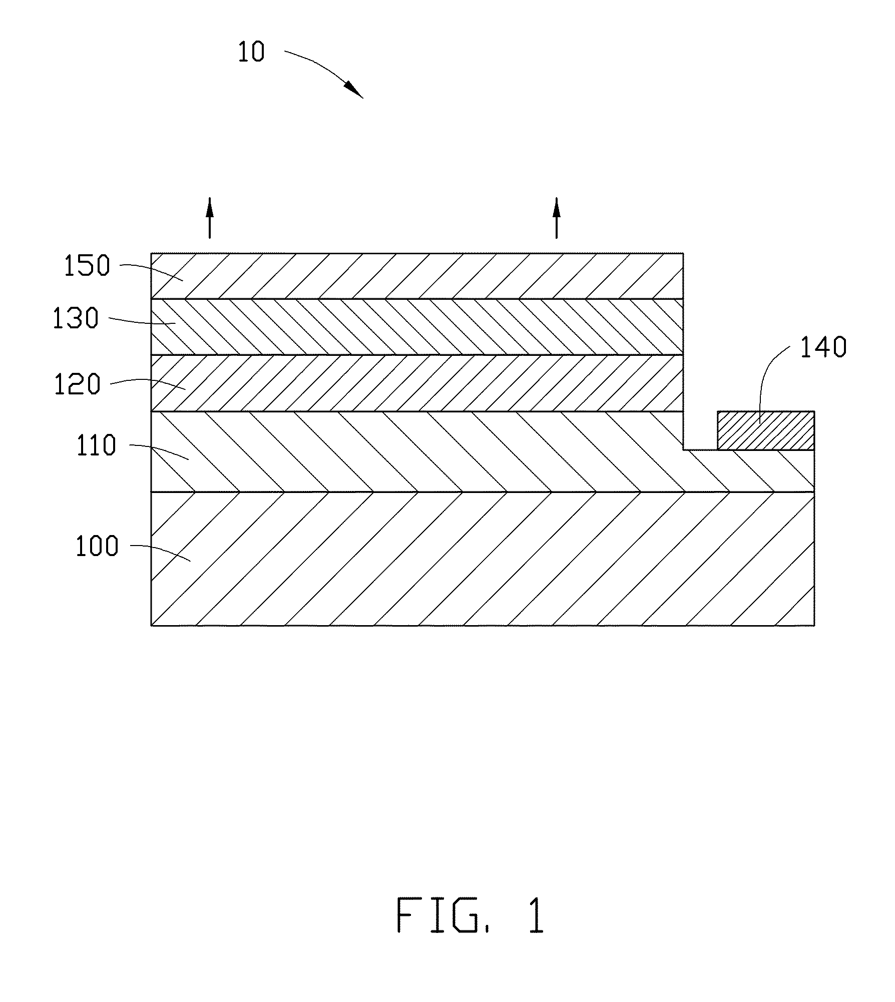
[0021]Referring to FIG. 1, one embodiment of an LED 10 includes a substrate 100, a first semiconductor layer 110, an active layer 120, a second semiconductor layer 130, a first electrode 140, and a second electrode 150. The first semiconductor layer 110, the active layer 120, the second semiconductor layer 130, the first electrode 140, and the second electrode 150 are stacked on the substrate 100. The first semiconductor layer 110 is in contact with the substrate 100. The active layer 120 is sandwiched between the first semiconductor layer 110 and the second semiconductor layer 130. A surface of the second semiconductor layer 130 away from the ac...


PUM

PropertyMeasurementUnit
distanceaaaaaaaaaa
diameteraaaaaaaaaa
distanceaaaaaaaaaa

Abstract

A light emitting diode includes a first semiconductor layer, an active layer, a second semiconductor layer, a first electrode, a second electrode. The second electrode includes a treated patterned carbon nanotube film. The treated patterned carbon nanotube film includes at least two carbon nanotube linear units spaced from each other; and carbon nanotube groups spaced from each other. The carbon nanotube groups are located between the at least two carbon nanotube linear units, and combined with the at least two carbon nanotube linear units.

Description

RELATED APPLICATIONS[0001]This application claims all benefits accruing under 35 U.S.C. §119 from China Patent Application No. 201210368199.4, filed on Sep. 28, 2012 in the China Intellectual Property Office, the disclosure of which is incorporated herein by reference. This application is related to a commonly-assigned application entitled, “ORGANIC LIGHT EMITTING DIODE,”.BACKGROUND[0002]1. Technical Field[0003]The present disclosure relates to a light emitting diode.[0004]2. Discussion of Related Art[0005]Semiconductor structures fabricated by gallium nitride for light sources, such as blue, green, and white light sources, have long lifetime, high energy conversion efficiency, and green. Therefore, the semiconductor structures are widely used as the light sources in large screen color display systems, automotive lightening, traffic lights, multimedia displays, optical communication systems, and so on.[0006]A standard light emitting diode (LED) includes an N-type semiconductor layer...

Claims


Application Information

Patent Timeline
Patent Type & Authority Patents(United States)
IPC IPC(8): H01L29/12B82Y20/00B82Y30/00B82Y99/00H01L29/06H01L33/40H01L33/42H01L51/00H01L51/52
CPCH01L33/40H01L33/42Y10S977/742B82Y99/00H01L29/0673H01L51/0048H01L51/5203B82Y30/00B82Y20/00H10K50/805H10K85/221
Inventor FENG, CHENQIAN, LIWANG, YU-QUAN
Owner BEIJING FUNATE INNOVATION TECH
Why Eureka
Try Eureka