
Method for extracting critical dimension of semiconductor nanostructure

a critical dimension and semiconductor nanotechnology, applied in the field of semiconductor nanostructure extraction, can solve the problems of increasing the requirement for parameter accuracy to be extracted, no good global optimal result can be obtained, and the simulation parameters are expanded, so as to facilitate accurate and fast extraction of feature linewidth and process simple

Active Publication Date: 2015-06-30
HUAZHONG UNIV OF SCI & TECH
View PDF3 Cites 0 Cited by
  • Summary
  • Abstract
  • Description
  • Claims
  • Application Information

AI Technical Summary

Benefits of technology

[0008]In view of the above-described problems, it is one objective of the invention to provide a method for extracting a critical dimension of a semiconductor nanostructure capable of facilitating accurate and fast extraction of feature linewidth, height, and sidewall angles, and featuring a simple process.
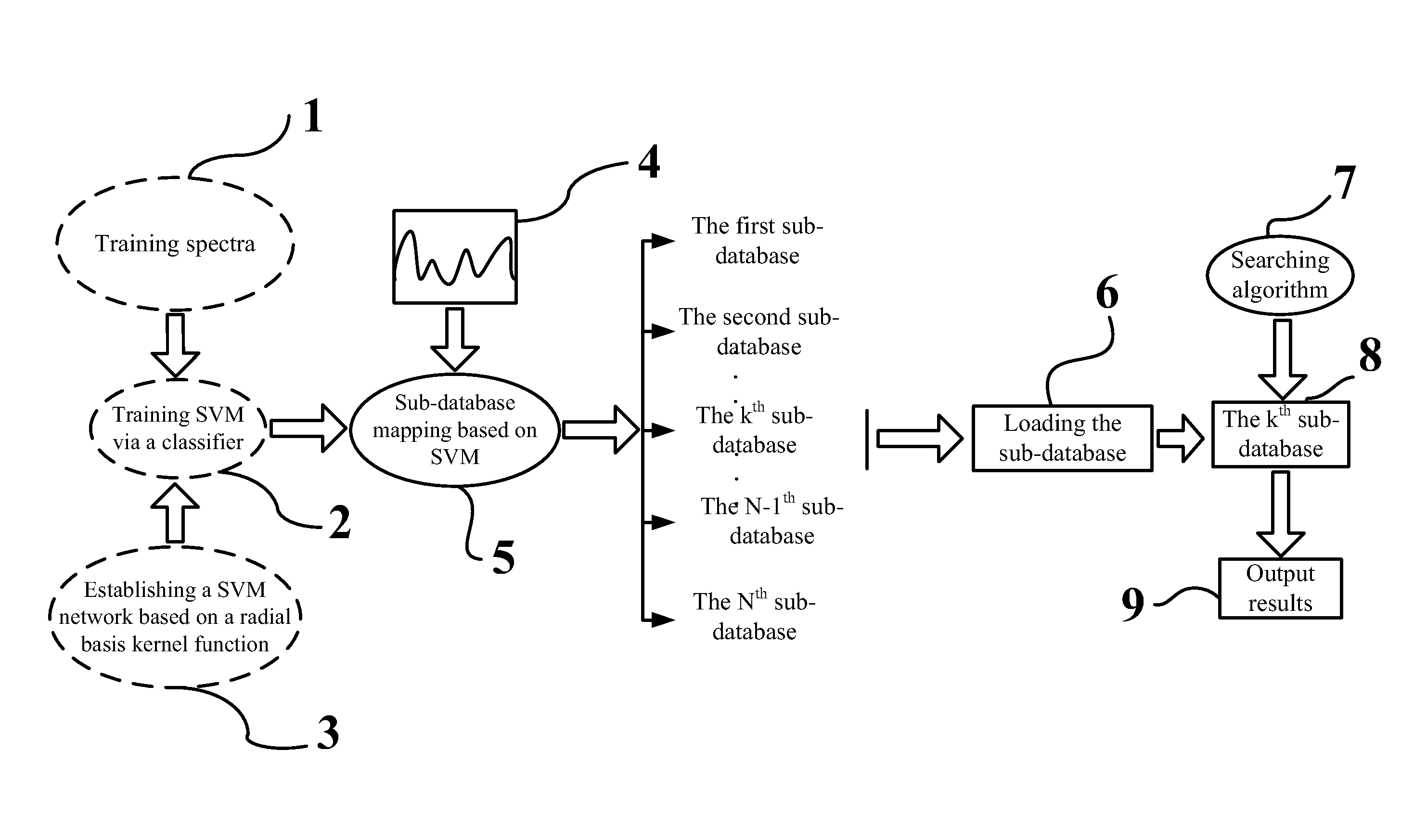
[0023]Advantages of the method for extracting a critical dimension of a semiconductor nanostructure are summarized below. Compared with a library-mapping-based method for extracting feature dimensions in the prior art, the invention is capable of mapping the measured spectra into a small-range sub-database by adding a process of off-line training using a SVM classifier, and time spent on searching in the sub-database is far less than that on most-similar spectra searching in a large database. In addition, by increasing the number of categories in each classifier (namely dividing value range for each parameter into multiple sub-ranges), a smaller sub-database can be obtained, which further accelerates extraction of the parameters, and the invention also implements predicable and controllable extraction speed of the parameters.

Problems solved by technology

However, the spectra database often includes large amount of simulation spectra, and the number of the spectra is to grow in a geometrical progression with increase of parameters of the nano structures, expansion of simulation parameters, and rise in requirement for accuracy of parameters to be extracted.
Searching in a database includes searching for a simulation spectrum most similar to a measured spectrum in the database according to certain rules, and is a typical problem of maximum proximity searching.
However, no good global optimal result can be obtained when the above-mentioned methods, except for the whole-library searching method, are used to solve problems such as most-similar spectra searching.
However, problems with this method are that, with further expansion of the simulation spectra database, more powerful and high-efficient GPUs must be used, which limits scalability of this category of hardware-acceleration-based searching method.

Method used


Image

  • Method for extracting critical dimension of semiconductor nanostructure
  • Method for extracting critical dimension of semiconductor nanostructure
  • Method for extracting critical dimension of semiconductor nanostructure

Examples


Embodiment Construction

[0030]For further illustrating the invention, experiments detailing a method for extracting a critical dimension of a semiconductor nanostructure are described below. It should be noted that the following examples are intended to describe and not to limit the invention.

[0031]As shown in FIG. 1, a method for extracting a critical dimension of a semiconductor nanostructure of the invention comprises steps of (take a one-dimensional trapezoid grating structure as an example):

[0032](1) determining parameters to be extracted of a one-dimensional trapezoid grating structure, and value ranges thereof;

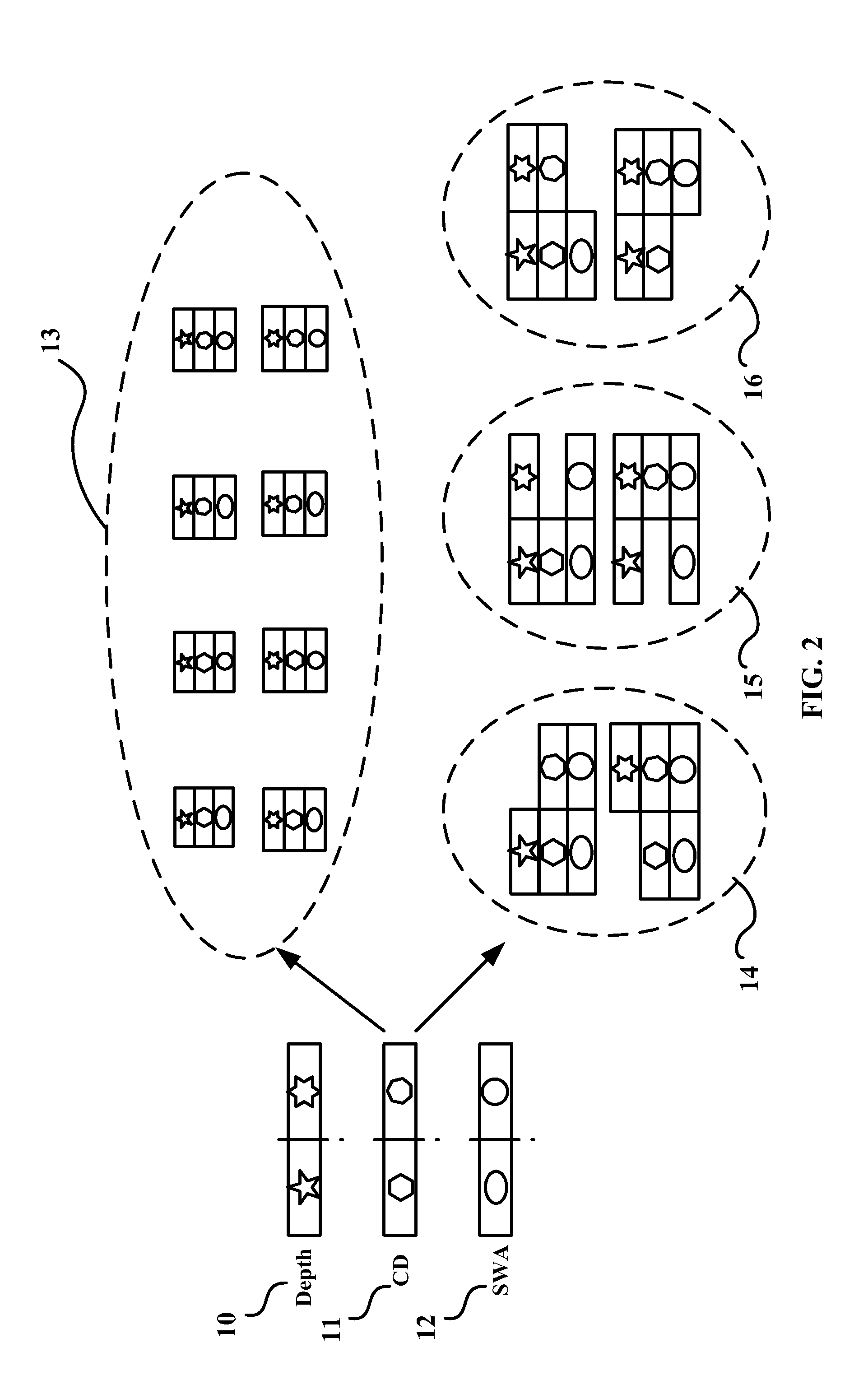
[0033]As shown in FIG. 3, a linewidth (w), a line height (depth) and a sidewall angle (SWA) are three parameters to be extracted.

[0034]As shown in FIG. 2, lengths of three rectangles 10, 11 and 12 are respectively used to represent value ranges of the linewidth (w), the line height (depth) and the sidewall angle (SWA).

[0035](2) dividing the value ranges of the parameters whereby obtaining diff...


PUM


Abstract

A method for extracting a critical dimension of a semiconductor nanostructure. The method includes: 1) determining a value range for each parameter to be extracted, whereby generating an electronic spectra database, and employing training spectra and support vector machine (SVM) training networks for training of SVMs; 2) employing the SVMs after training to map measured spectra to yield a corresponding electronic spectra database; and 3) employing a searching algorithm to search for an optimum simulation spectrum in the corresponding electronic spectra database, simulation parameters corresponding to the simulation spectrum being the critical dimension of the semiconductor nanostructure to be extracted.

Description

CROSS-REFERENCE TO RELATED APPLICATIONS[0001]Pursuant to 35 U.S.C. §119 and the Paris Convention Treaty, this application claims the benefit of Chinese Patent Application No. 201210177237.8 filed on May 31, 2012, the contents of which, including any intervening amendments thereto, are incorporated herein by reference. Inquiries from the public to applicants or assignees concerning this document or the related applications should be directed to: Matthias Scholl P.C., Attn.: Dr. Matthias Scholl Esq., 14781 Memorial Drive, Suite 1319, Houston, Tex. 77079.BACKGROUND OF THE INVENTION[0002]1. Field of the Invention[0003]The invention relates to a semiconductor and optical scattering measurement field, and more particularly, to a method for extracting a critical dimension of a semiconductor nanostructure.[0004]2. Description of the Related Art[0005]For the purpose of implementing operability, repeatability, and extendibility of nano manufacturing process, and ensuring reliability, uniformi...

Claims


Application Information

Patent Timeline
Patent Type & Authority Patents(United States)
IPC IPC(8): G06N5/00G06N99/00G06F1/00G06N20/10
CPCG06N99/005G06N20/00G06N20/10
Inventor LIU, SHIYUANZHU, JINLONGZHANG, CHUANWEICHEN, XIUGUO
Owner HUAZHONG UNIV OF SCI & TECH
Learn More