
Thin film transistor, display substrate and method of manufacturing a thin film transistor

a technology of thin film transistor and display substrate, which is applied in the direction of transistors, semiconductor devices, electrical devices, etc., can solve the problems of high manufacturing cost and uniform polycrystalline silicon layer, and achieve the effect of improving reliability

Active Publication Date: 2015-06-30
SAMSUNG DISPLAY CO LTD
View PDF11 Cites 3 Cited by
  • Summary
  • Abstract
  • Description
  • Claims
  • Application Information

AI Technical Summary

Benefits of technology

The solution provides improved reliability and high electron mobility of about 10 to 40 cm2 / V·s, maintaining uniform electrical characteristics and resisting changes during manufacturing, thus enhancing the performance and durability of the thin film transistor.

Problems solved by technology

Thus, forming a uniform polycrystalline silicon layer on a large-sized substrate may be difficult, and resulting manufacturing costs are high.

Method used


Image

  • Thin film transistor, display substrate and method of manufacturing a thin film transistor
  • Thin film transistor, display substrate and method of manufacturing a thin film transistor
  • Thin film transistor, display substrate and method of manufacturing a thin film transistor

Examples


experiment 1

Forming an IZTO layer

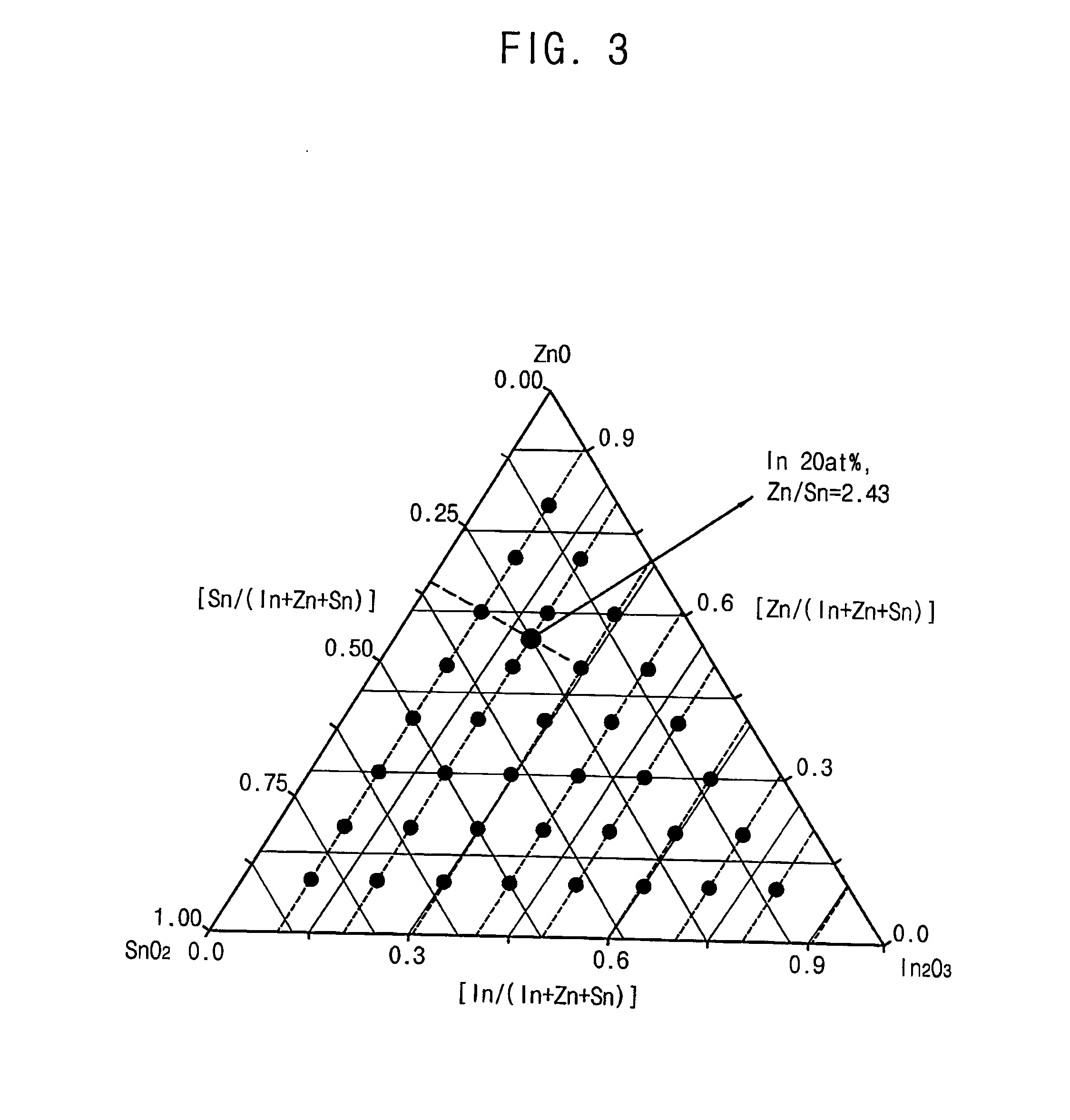
[0100]Targets having IZTO were prepared according to the following Table 1. Through electron probe micro analysis, the targets of Examples 1 and 2 were confirmed to have a uniform single phase, and the target of Comparative Example 1 was confirmed to have a multiple phase. Semiconductor layers including IZTO were formed through a sputtering process using the targets of Examples 1 and 2 and Comparative Example 1. Thereafter, the semiconductor layers were annealed at about 300° C. for about 1 hour. Composition variation of the semiconductor layers are detailed in the following Table 1.

[0101]

TABLE 1Composition ofComposition ofTargetsemiconductor layersemiconductor layercompositionbefore annealingafter annealing(In:Zn:Sn)(In:Zn:Sn)(In:Zn:Sn)Example 120:56.7:23.321.9:51.5:26.721.8:51.5:26.7Example 213:60:2714:55:3114:55:31Comparative20:48:3219.8:47.6:32.519.3:46.2:34.5Example 1

[0102]Referring to Table 1, composition of the semiconductor layers of Examples 1 and 2 was...

experiment 2

Forming a Thin Film Transistor

[0105]A thin film transistor including a semiconductor layer including IZTO and having a thickness of about 500 Å. The thin film transistor was annealed at about 300° C. for about 1 hour.

[0106]An electron mobility of the thin film transistor was about 22.41 cm2 / V·s. Furthermore, a shift value of a threshold voltage of the thin film transistor was no more than about 3.5 volts (V) when the thin film transistor was exposed to a light of about 25,000 nit at about 60° C. for about 1 hour.

[0107]Thus, it can be noted that an exemplary embodiment of a thin film transistor manufactured according to the invention may have high electron mobility and reliability.

[0108]Exemplary embodiments of the invention may be used for a display device such as a LCD or an OLED display device.


PUM


Abstract

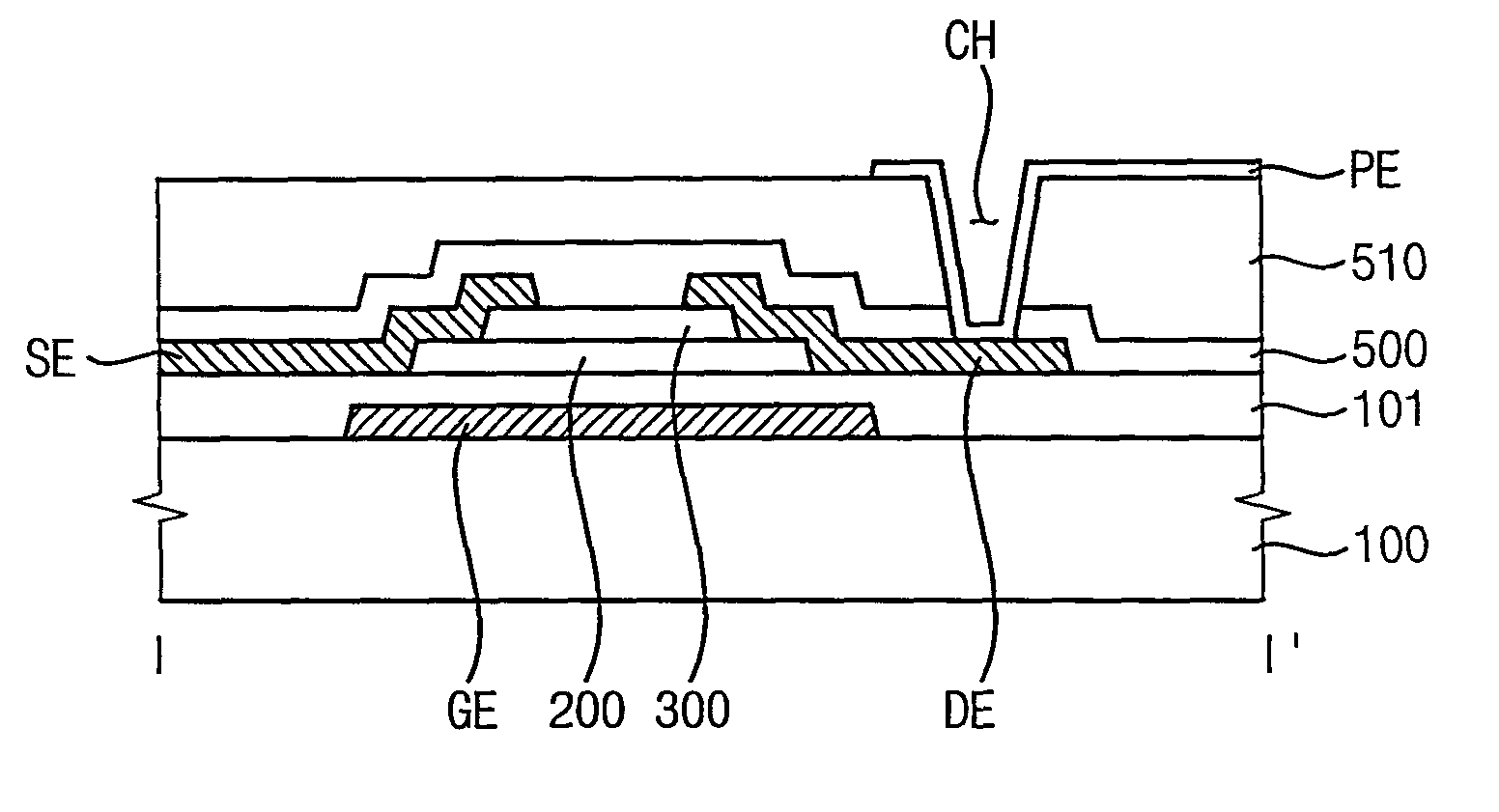
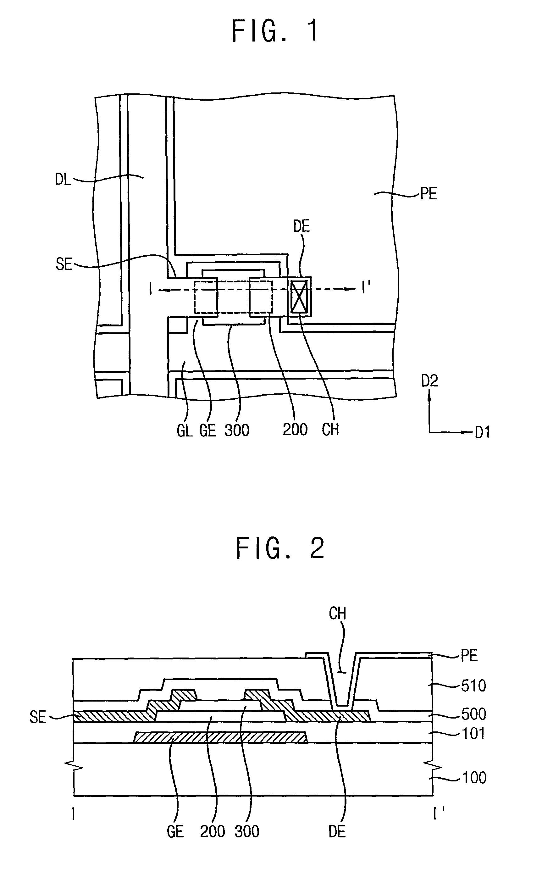
A thin film transistor includes a gate electrode, a channel overlapped with the gate electrode, a source electrode contacting the channel, and a drain electrode spaced apart from the source electrode and contacting the channel. The channel includes indium-zinc-tin oxide sourced from a source including a single phase indium-zinc-tin oxide.

Description

[0001]This application claims priority to Korean Patent Application No. 10-2013-0058272, filed on May 23, 2013, and all the benefits accruing therefrom under 35 U.S.C. §119, the contents of which application are herein incorporated by reference in their entirety.BACKGROUND[0002]1. Field[0003]The invention relates to a thin film transistor. More particularly, the invention relates to a thin film transistor including an oxide semiconductor, a display substrate including the thin film transistor and a method of manufacturing the thin film transistor.[0004]2. Description of Related Art[0005]Generally, a thin film transistor for driving a pixel in a display device includes a gate electrode, a source electrode, a drain electrode, and an active pattern forming a channel between the source electrode and the drain electrode. The active pattern includes a semiconductor layer including amorphous silicon, polycrystalline silicon, oxide semiconductor, or the like.[0006]Amorphous silicon has a re...

Claims


Application Information

Patent Timeline
Patent Type & Authority Patents(United States)
IPC IPC(8): H01L29/00H01L29/786H01L27/12H01L29/66
CPCH01L27/1225H01L29/78693H01L29/66969H01L29/78633H01L21/02554H01L21/02565H01L29/66742
Inventor AHN, BYUNG-DUKIM, GUN-HEELIM, JUN-HYUNGKUGIMIYA, TOSHIHIROGOTO, HIROSHIMIKI, AYAMORITA, SHINYA
Owner SAMSUNG DISPLAY CO LTD
Learn More