
Display panel and preparation method thereof

A display panel and display area technology, which is applied in semiconductor/solid-state device manufacturing, semiconductor devices, electrical components, etc., can solve the problem that silver electrodes of metal lines are easily oxidized and corroded, reduce the reliability of OLED backplanes, and change contact resistance. Large and other problems, to achieve the effect of improving reliability and product quality, strong acid resistance and good stability

Active Publication Date: 2021-06-04
SHENZHEN CHINA STAR OPTOELECTRONICS SEMICON DISPLAY TECH CO LTD
View PDF7 Cites 2 Cited by
  • Summary
  • Abstract
  • Description
  • Claims
  • Application Information

AI Technical Summary

Problems solved by technology

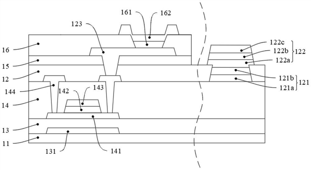
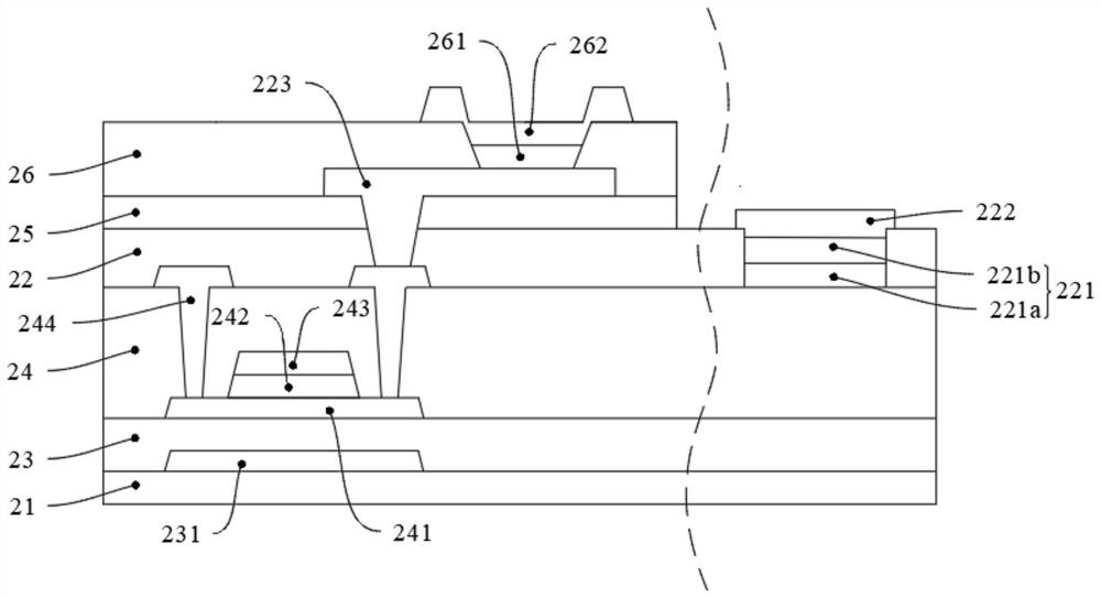
[0006] Embodiments of the present invention provide a display panel and a method for preparing the display panel, which are used to solve the problem in the prior art that the silver electrodes of the metal wires in the binding area are easily oxidized and corroded, resulting in weak binding areas and reduced contact resistance. Large, thereby reducing technical issues such as OLED backplane reliability

Method used


Image

  • Display panel and preparation method thereof
  • Display panel and preparation method thereof
  • Display panel and preparation method thereof

Examples


Embodiment Construction

[0038] The following will clearly and completely describe the technical solutions in the embodiments of the present invention with reference to the drawings in the embodiments of the present invention. Apparently, the described embodiments are only some of the embodiments of the present invention, but not all of them. Based on the embodiments of the present invention, all other embodiments obtained by those skilled in the art without creative efforts fall within the protection scope of the present invention.

[0039] In describing the present invention, it should be understood that the terms "center", "longitudinal", "transverse", "length", "width", "thickness", "upper", "lower", "front", " Orientation indicated by rear, left, right, vertical, horizontal, top, bottom, inside, outside, clockwise, counterclockwise, etc. The positional relationship is based on the orientation or positional relationship shown in the drawings, which is only for the convenience of describing the pr...


PUM


Abstract

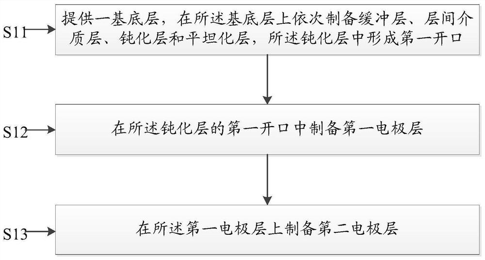
The invention discloses a display panel and a preparation method thereof, and the display panel comprises the components of a substrate layer which comprises a display area and a non-display area which is arranged around the display area; a passivation layer which is arranged on one side of the substrate layer, wherein a first opening is formed in the passivation layer, and the first opening is located in the non-display area; a first electrode layer which is arranged on one side, close to the substrate layer, in the first opening of the passivation layer; and a second electrode layer which is arranged on the surface of one side, far away from the substrate layer, of the first electrode layer, wherein the second electrode layer comprises a second electrode, and the material of the second electrode comprises at least one of indium gallium tin oxide, indium gallium zinc tin oxide and gallium tin oxide. According to the invention, the second electrode layer is arranged, the first electrode layer is prevented from making contact with oxygen to generate oxidation reaction, meanwhile, the silver electrode is etched away, oxidation reaction of the silver electrode is also avoided, and then the reliability and the product quality of the display panel are improved.

Description

technical field [0001] The invention relates to the field of display technology, in particular to a display panel and a method for preparing the display panel. Background technique [0002] At present, the development of OLED (Organic Light Emitting Diode, organic light emitting diode) display technology is advancing by leaps and bounds. Due to the advantages of light and thin, fast response, wide viewing angle, high contrast, and bendability, OLED products have received more and more attention and applications. Applied in display fields such as mobile phones, tablets, and TVs. [0003] In the top-emitting OLED structure, the commonly used ITO (Indium Tin Oxide, indium tin oxide) / Ag (silver) / ITO composite film layer can be used as the reflective layer and the anode electrode layer; ITO / Ag / ITO is connected to the OLED light-emitting device structure ; In the COF (Chip On Film, the integrated circuit is bound to the flexible circuit board) bonding (binding) area of ​​the back...

Claims


Application Information

Patent Timeline
IPC IPC(8): H01L51/52H01L51/56H01L27/32
CPCH10K59/131H10K50/805H10K71/00
Inventor 胡小波
Owner SHENZHEN CHINA STAR OPTOELECTRONICS SEMICON DISPLAY TECH CO LTD
Learn More