Composite film electrode based on low-cost metal and transparent conductive oxide and application of composite film electrode in perovskite photoelectric device
A composite thin film, transparent and conductive technology, which is applied in the manufacture of electrical solid devices, semiconductor devices, semiconductor/solid devices, etc., can solve the problems of device efficiency decline, battery internal resistance increase, easy diffusion, etc., and achieve excellent conductivity and stability performance, high photoelectric conversion efficiency, and improved humidity stability
- Summary
- Abstract
- Description
- Claims
- Application Information
AI Technical Summary
Problems solved by technology
Method used
Image

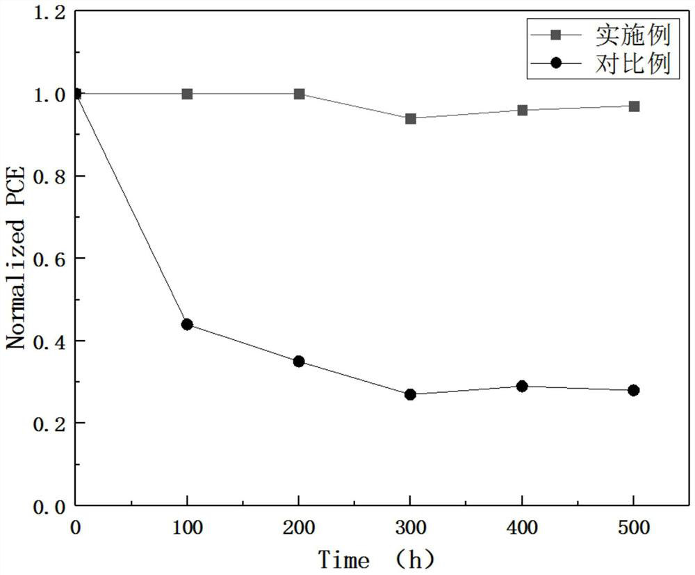
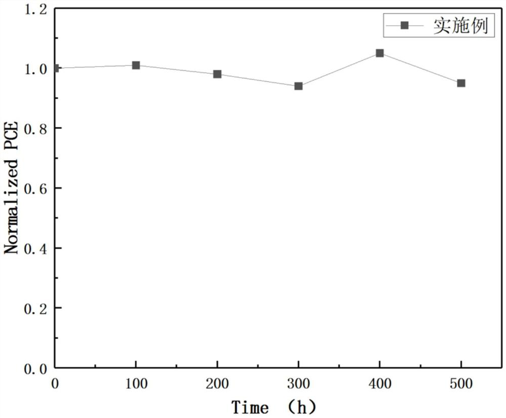
Examples
Embodiment 1
[0031] Embodiment 1, prepare perovskite solar cell
[0032] (1) Preparation of electron transport layer on transparent conductive oxide substrate
[0033] The tin oxide solution was spin-coated on the transparent conductive oxide substrate with a thickness of about 30 nm.
[0034] (2) Preparation of perovskite layer on the electron transport layer
[0035] will FA 0.9 MA 0.1 PB 3 The perovskite precursor solution is spin-coated on the electron transport layer with a thickness of about 600 nm.
[0036] (3) Preparation of a hole transport layer on the perovskite layer
[0037] The hole-transporting material Spiro-OMeTAD is spin-coated on the perovskite layer by solution spin-coating, with a thickness of about 150 nm.
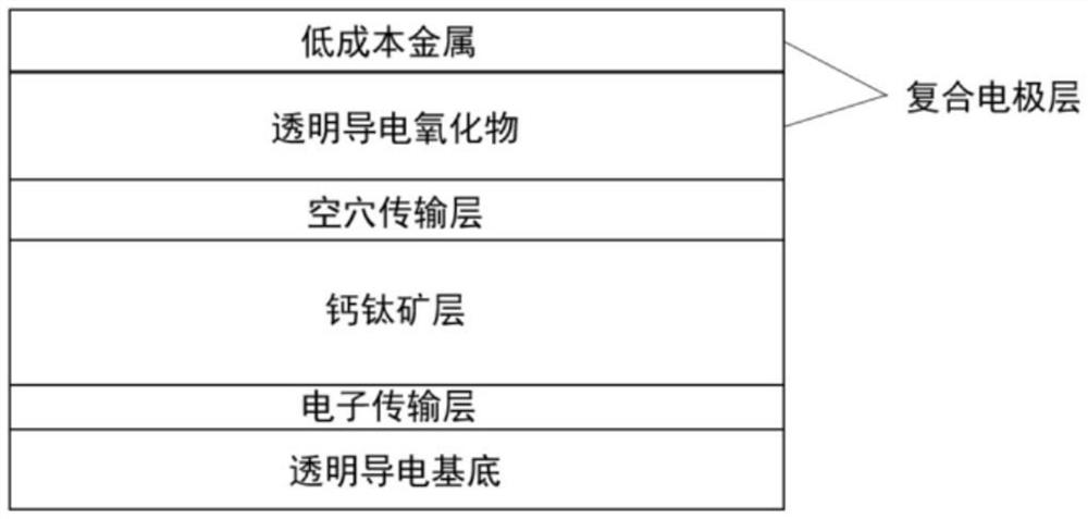
[0038] (4) Preparation of a composite electrode layer on the hole transport layer
[0039] First, molybdenum oxide with a thickness of about 10 nm is thermally evaporated on the hole transport layer as a buffer layer in the magnetron sputtering process; the...
Embodiment 2
[0042] Embodiment 2, prepare perovskite solar cell
[0043] (1) Preparation of electron transport layer on transparent conductive oxide substrate
[0044] The tin oxide solution was spin-coated on the transparent conductive oxide substrate with a thickness of about 30 nm.
[0045] (2) Preparation of perovskite layer on the electron transport layer
[0046] will FA 0.9 MA 0.1 PB 3 The perovskite precursor solution is spin-coated on the electron transport layer with a thickness of about 600 nm.
[0047] (3) Preparation of a hole transport layer on the perovskite layer
[0048] The hole-transporting material Spiro-OMeTAD is spin-coated on the perovskite layer by solution spin-coating, with a thickness of about 150 nm.
[0049] (4) Preparation of a composite electrode layer on the hole transport layer
[0050]First, molybdenum oxide with a thickness of about 10 nm is thermally evaporated on the hole transport layer as a buffer layer in the magnetron sputtering process; then...
Embodiment 3
[0052] Embodiment 3, preparation perovskite solar cell
[0053] (1) Preparation of electron transport layer on transparent conductive oxide substrate
[0054] The tin oxide solution was spin-coated on the transparent conductive oxide substrate with a thickness of about 30 nm.
[0055] (2) Preparation of perovskite layer on the electron transport layer
[0056] will FA 0.9 MA 0.1 PB 3 The perovskite precursor solution is spin-coated on the electron transport layer with a thickness of about 600 nm.
[0057] (3) Preparation of a hole transport layer on the perovskite layer
[0058] The hole-transporting material Spiro-OMeTAD is spin-coated on the perovskite layer by solution spin-coating, with a thickness of about 150 nm.
[0059] (4) Preparation of a composite electrode layer on the hole transport layer
[0060] First, molybdenum oxide with a thickness of about 10nm is thermally evaporated on the hole transport layer as a buffer layer in the magnetron sputtering process; ...
PUM
| Property | Measurement | Unit |
|---|---|---|
| thickness | aaaaa | aaaaa |
| thickness | aaaaa | aaaaa |
| thickness | aaaaa | aaaaa |
Abstract
Description
Claims
Application Information
 - R&D
- Intellectual Property
- Life Sciences
- Materials
- Tech Scout
- Unparalleled Data Quality
- Higher Quality Content
- 60% Fewer Hallucinations
Browse by: Latest US Patents, China's latest patents, Technical Efficacy Thesaurus, Application Domain, Technology Topic, Popular Technical Reports.
© 2025 PatSnap. All rights reserved.Legal|Privacy policy|Modern Slavery Act Transparency Statement|Sitemap|About US| Contact US: help@patsnap.com