Semiconductor device and method of manufacturing same

a semiconductor and semiconductor technology, applied in the direction of semiconductor devices, semiconductor/solid-state device details, electrical apparatus, etc., can solve the problems of inability to achieve sufficient long-term reliability of solder joints, unstable positions for joining them together, and damage to the electric connection of semiconductor devices, etc., to achieve efficient release of heat from and reduce the shelf life of the solder layer. , the effect of easy and reliable position of the lead frame and solder pla

Active Publication Date: 2015-07-07
FUJI ELECTRIC CO LTD
View PDF16 Cites 2 Cited by
  • Summary
  • Abstract
  • Description
  • Claims
  • Application Information

AI Technical Summary

Benefits of technology

[0018]The present invention can easily and reliably position the lead frame and solder plates at the same time without using a conventional positioning frame body. In addition, efficient release of heat from the lead frame can be achieved without reducing the shelf life of the solder layers through which the lead frame is joined to the insulating substrate. The present invention, therefore, can provide a semiconductor device of improved reliability and ease of assembly associated with the increased current and downsizing thereof.

Problems solved by technology

This can cause cracks on the periphery of each solder layer, damaging the electric connection in the semiconductor device.
Or when the area for a solder fillet becomes insufficient, sufficient long-term reliability of the solder joints cannot be achieved because of thermal stress.
As described above, the problem in assembling the lead frame of the conventional semiconductor device is difficulty in positioning the metal plate 18 and the like on the insulating substrate 10, therefore, positions for joining them together is unstable.

Method used


Image

  • Semiconductor device and method of manufacturing same
  • Semiconductor device and method of manufacturing same
  • Semiconductor device and method of manufacturing same

Examples


first embodiment

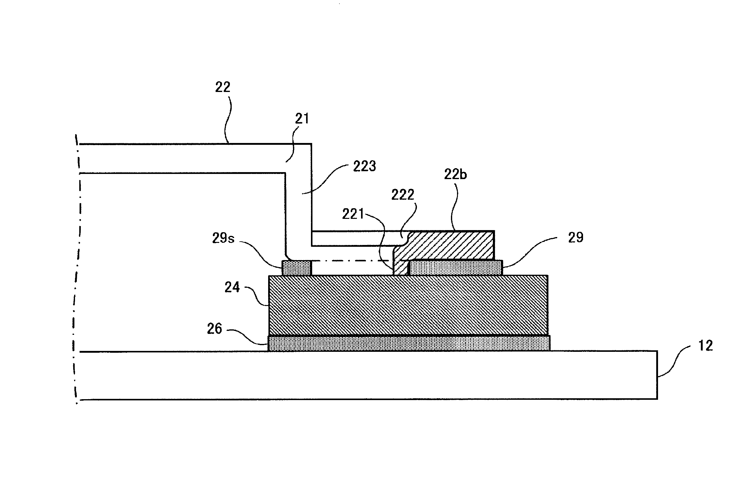
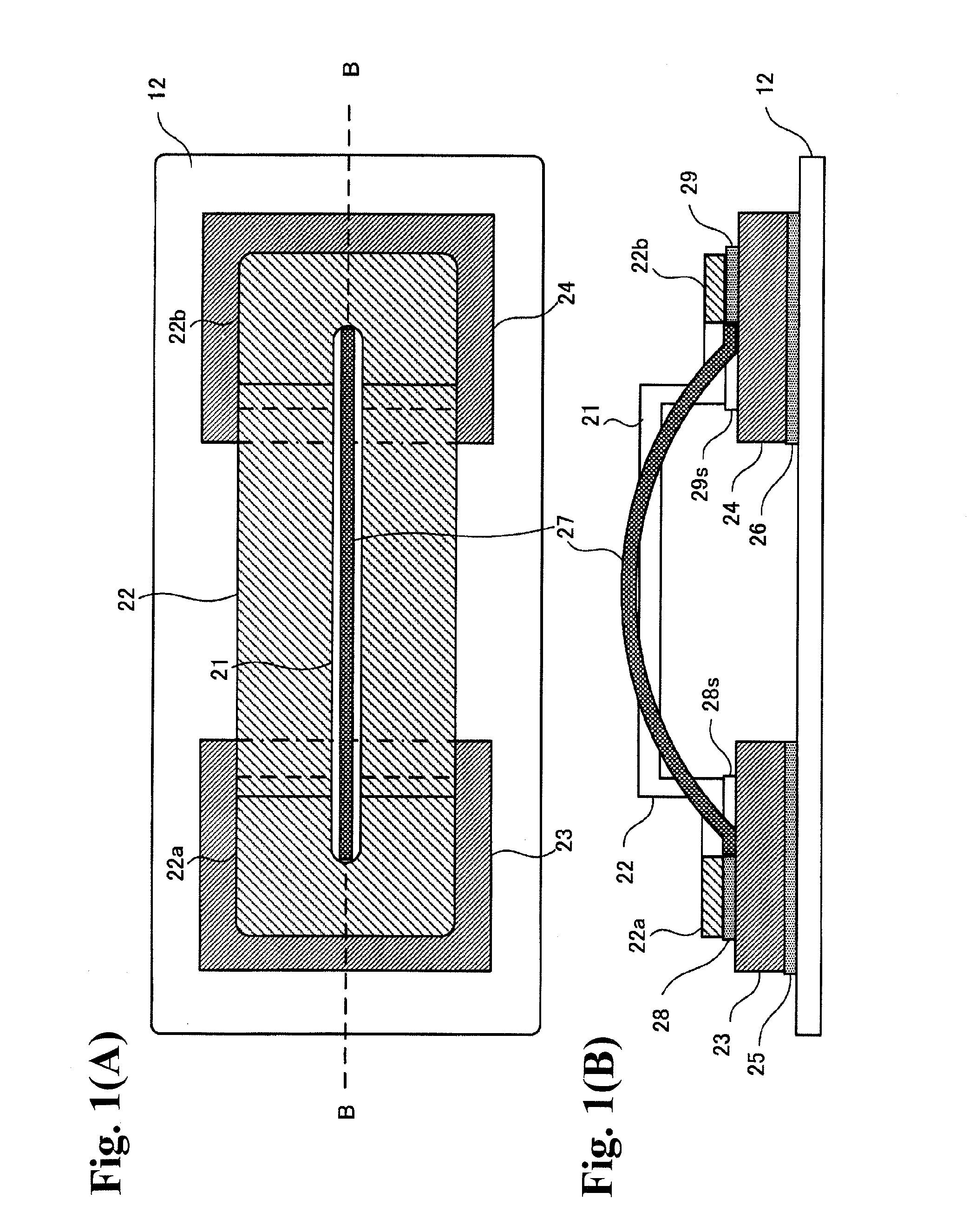
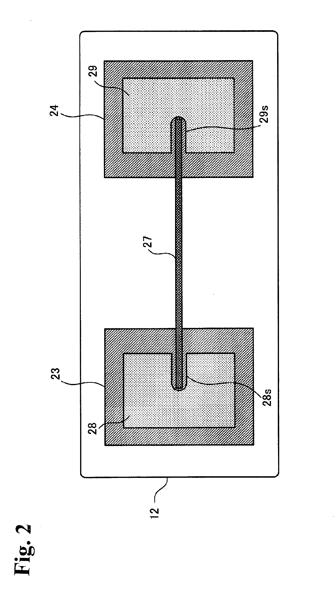
[0033]FIGS. 1(A), 1(B) are diagrams showing an example of a semiconductor device according to a first embodiment, where FIG. 1(A) is a plan view of the semiconductor device and FIG. 1(B) is a cross-sectional view taken along the line B-B.

[0034]This semiconductor device is configured such that electronic components 23, 24 on an insulating substrate (not shown) formed with a metal layer constituting a conductive pattern 12 are electrically connected to each other by a rectangular lead frame 22 having an opening 21. The lead frame has joints 22a, 22b which are sized corresponding to electrode surfaces of the electronic components 23, 24, at left and right ends of the lead frame, and, as shown in FIG. 1(B), these joints 22a, 22b electrically connect the electronic components 23, 24 to each other via rising portions of a predetermined height provided in the lead frame 22. The opening of the lead frame 22 is formed as a long hole having a predetermined width and a length equivalent to the...

second embodiment

[0051]FIGS. 6(A), 6(B) are diagrams showing an example of a semiconductor device according to a second embodiment, where FIG. 6(A) is a plan view of the semiconductor device and FIG. 6(B) is a cross-sectional view taken along the line B-B. FIG. 7 is a diagram showing an equivalent circuit of the semiconductor device according to the second embodiment.

[0052]In the semiconductor device shown in these diagrams, an insulating substrate formed of a ceramic substrate 11 is joined / mounted onto a several millimeter thick metal base plate via a tin (Sn)-silver (Ag) based lead-free solder layer (not shown). Power semiconductor elements such as IGBT chips 23a, 23b and diode chips 24a, 24b are loaded on the ceramic substrate 11. In this semiconductor device, the power semiconductor elements, the insulating substrate and the like are packaged in a resin case to configure an all-purpose IGBT module. A power semiconductor element module normally has a two-in-one structure formed of two elements of...

third embodiment

[0064]FIGS. 10(A)-10(C) are diagrams showing an example of a lead frame used in a semiconductor device according to a third embodiment, wherein FIG. 10(A) is a plan view of the lead frame, FIG. 10(B) is a cross-sectional view taken along the line B-B, and FIG. 10(C) is a partial cross-sectional enlarged view.

[0065]In place of the long holes of the lead frame 33 shown in FIGS. 8(A), 8(B), stepped round holes ha1, ha2, hb1 to hb5, hc1, and hc2 are formed in such a manner as to penetrate through joints 35a to 35c in this lead frame 35. As shown in the enlarged cross-sectional view of FIG. 10(C), a projection 351 projecting downward is formed on the back of the stepped round hole ha2 (on the side joined to the insulating substrate). A step portion 352 is formed on the front side of the stepped round hole ha2. Note that the height H of the projection 351 is equivalent to the thickness of a solder plate used as a joining material.

[0066]In this case as well, the lead frame 35 can easily be...


PUM


Abstract

A semiconductor device has a plurality of electronic components mounted on an insulating substrate formed with a metal layer, and electrically connected to each other or to the metal layer; a positioning wire member having a predetermined diameter and a predetermined length, and bonded to each of the plurality of electronic components or to the metal layer; a lead frame disposed to bridge and electrically connect the plurality of electronic components to each other or between the metal layer and the electronic components; and an opening having a size capable of inserting the wire member therethrough formed to penetrate through the lead frame, to join the lead frame to each of the electronic components or the metal layer at a predetermined position therein. The lead frame is positioned on the insulating substrate by inserting the wire member into the opening.

Description

RELATED APPLICATIONS[0001]The present application is National Phase of International Application No. PCT / JP2012 / 065224 filed Jun. 14, 2012, and claims priority from Japanese Applications No. 2011-174540 filed Aug. 10, 2011.TECHNICAL FIELD[0002]The present invention relates to a semiconductor device having a module structure in which a plurality of electronic components is mounted on an insulating substrate formed with a metal layer, and a method of manufacturing such a semiconductor device. Particularly, the present invention relates to a semiconductor device that is configured by electrically connecting electronic components such as semiconductor chips on an insulating substrate to each other or to a metal layer, and relates to a method of manufacturing such a semiconductor device.BACKGROUND ART[0003]Among the semiconductor devices equipped with small, large-current electronic components, there is a semiconductor device in which semiconductor chips are fixed to a metal layer (condu...

Claims


Application Information

Patent Timeline
Patent Type & Authority Patents(United States)
IPC IPC(8): H01L23/495H01L25/07H01L23/00H01L23/498H01L23/373H01L23/24H01L23/31H01L25/18
CPCH01L23/49575H01L24/73H01L24/92H01L25/072H01L24/48H01L24/37H01L24/40H01L24/81H01L24/84H01L23/3735H01L23/49844H01L2224/48137H01L2224/73265H01L2224/32225H01L2224/48091H01L2924/01029H01L2224/40137H01L2224/40139H01L2224/40227H01L2224/37011H01L2224/45124H01L2224/45147H01L2224/48227H01L2224/73221H01L2224/85205H01L2224/92247H01L2924/13055H01L2224/92166H01L2224/48472H01L23/3107H01L24/32H01L24/45H01L24/83H01L24/85H01L25/18H01L2224/04026H01L2224/04034H01L2224/04042H01L2224/06181H01L2224/37147H01L2224/73263H01L2224/83815H01L2924/1203H01L2224/40993H01L2924/01015H01L2924/01047H01L24/06H01L24/29H01L2224/291H01L23/49524H01L23/24H01L2224/84138H01L2924/1305H01L2924/00014H01L2924/00H01L2924/01026H01L2924/01042H01L2924/014H01L2224/45015H01L2924/351H01L2924/15787H01L2224/40095H01L2224/40225H01L2924/00011H01L2224/77272H01L2224/0603H01L2224/4007H01L2224/40091H01L2224/48145H01L2224/48465H01L2224/85001H01L2224/84801H01L2924/2076H01L2924/00015H01L2224/83205H01L2924/00012H01L2224/85399H01L2224/05599
Inventor SOYANO, SHIN
Owner FUJI ELECTRIC CO LTD
Why Eureka
Try Eureka