Piezoelectric material and devices using the same

a piezoelectric element and piezoelectric material technology, applied in the field of piezoelectric elements, liquid discharge heads, ultrasonic motors, can solve the problems of polarizing bi, unclarified piezoelectric performance of lead components, and environmental impact of lead components

Active Publication Date: 2015-07-14
CANON KK +2
View PDF14 Cites 6 Cited by
  • Summary
  • Abstract
  • Description
  • Claims
  • Application Information

AI Technical Summary

Benefits of technology

[0058]Further, incorporating a moderate amount of Mn into the piezoelectric material of the present invention improves the insulation property of the piezoelectric material. A highly insulative piezoelectric material has an advantage in that the material can withstand polarization treatment under a high voltage, and is also excellent in conversion efficiency between electric energy and mechanical energy. In addition, incorporating a moderate amount of Mn into the piezoelectric material of the present invention exerts an effect by which the piezoelectric material can be polarized with an additionally low voltage.

Problems solved by technology

Therefore, the environmental impact of the lead component is considered to be a problem.
However, although the Bi(Zn0.5Ti0.5)O3 is theoretically expected to have excellent piezoelectric performance, it is difficult to polarize the Bi(Zn0.5Ti0.5)O3 due to its high Curie temperature, and hence the piezoelectric performance thereof has not been clarified.
However, there remains a problem that sufficient piezoelectric strain cannot be obtained from BiFeO3.
However, the piezoelectric performance of BiAlO3 has also not reached a practically applicable range yet.

Method used


Image

  • Piezoelectric material and devices using the same
  • Piezoelectric material and devices using the same
  • Piezoelectric material and devices using the same

Examples


examples 1 to 11 and 16 to 26

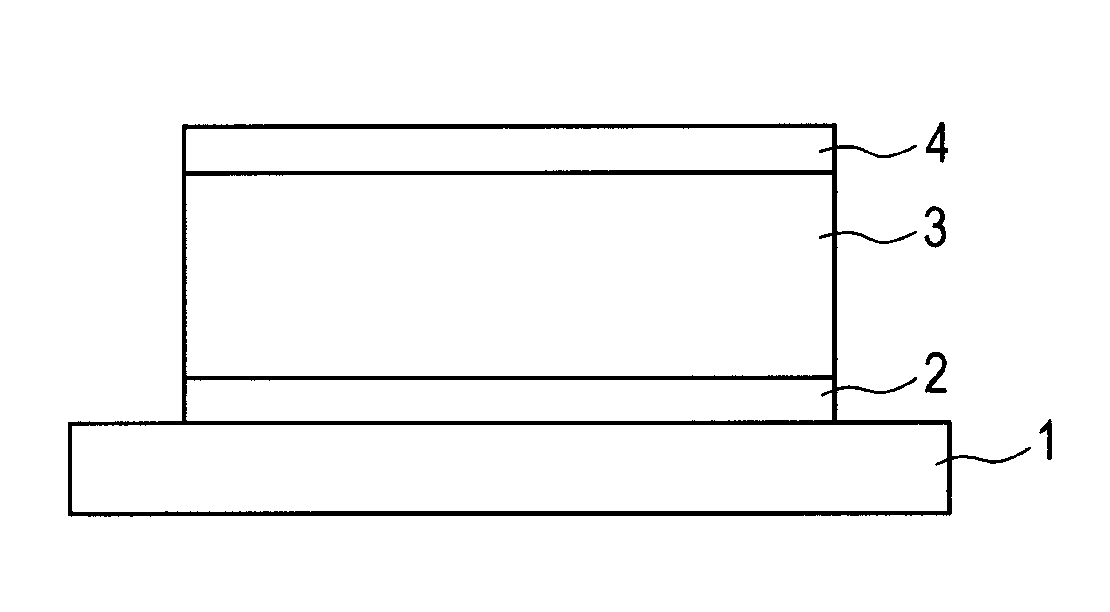
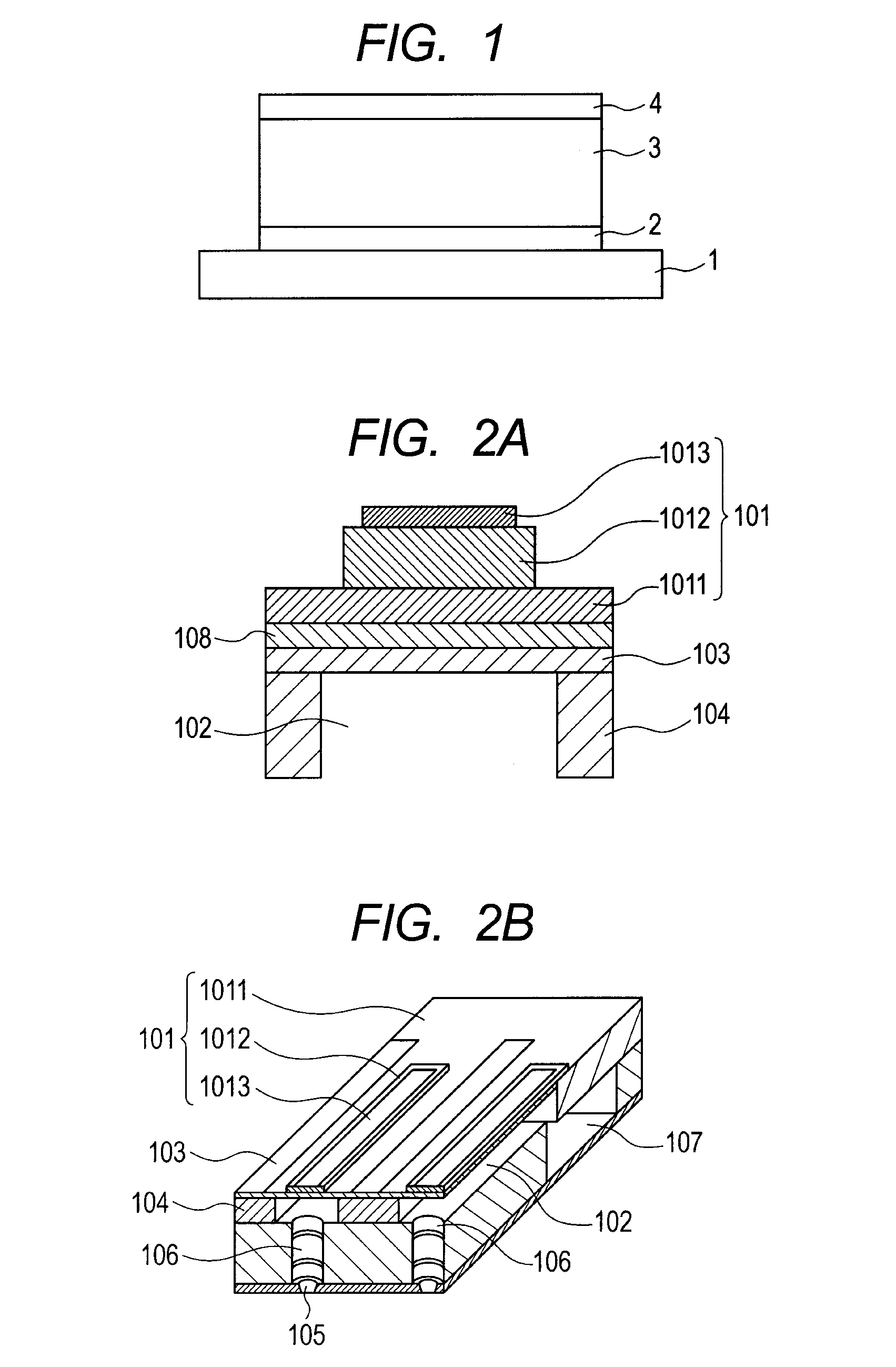
[0111]Metal oxide thin films having compositions corresponding to the respective examples of Table 1 and Table 3 were each formed on a substrate by an pulsed metal organic chemical vapor deposition method (MOCVD method).

[0112]A (100)-oriented strontium titanate (SrTiO3) single-crystal substrate having strontium ruthenate (SrRuO3) having a thickness of about 100 nm as a lower electrode on its film formation surface was used as the substrate on which any such thin film was formed. The SrRuO3 electrode was formed by a sputtering method.

[0113]There were used, as raw materials of the respective oxides of the metals, dimethyl(2-(N,N-dimethylaminomethyl)phenyl)bismuth (Bi(CH3)2(2-(CH3)2NCH2Ph)), tri(ethylpentadienyl)iron (Fe(C2H5C5H4)3), zinc bis(6-ethyl-2,2-dimethyl-3,5-decanedionate) (Zn(EDMDD)2), magnesium bis(2,2,6,6-tetramethyl-3,5-heptanedionate) (Mg(DPM)2), and tetra-i-propoxytitanium (Ti(O.i-Pr)4).

[0114]Nitrogen was used as a carrier gas, and oxygen and nitrogen were each used as a...

examples 12 and 27 to 41

[0128]Metal oxide thin films having compositions shown in Table 2 and Table 4 were each formed on a substrate by the MOCVD method in the same manner as in Examples 1 to 11 and 16 to 26.

[0129]A (110)-oriented strontium titanate (SrTiO3) single-crystal substrate having strontium ruthenate (SrRuO3) having a thickness of about 100 nm as a lower electrode on its film formation surface was used as the substrate on which any such thin film was formed. The SrRuO3 electrode was formed by a sputtering method.

[0130]There were used, as raw materials of the respective oxides of the metals, tri(2,2,6,6-tetramethyl-3,5-heptanedionate) (2,2-bipyridyl)lanthanum (La(TMOD)3bpy) and manganese tri(2,2,6,6,-tetramethyl-3,5-heptanedionate) (Mn(DPM)3), in addition to the raw materials used in Examples 1 to 11.

[0131]A thin film based on the piezoelectric material of the present invention having a thickness of 200 nm to 450 nm was obtained under the same film formation conditions as those of Examples 1 to 11...

examples 13 , 14

Examples 13, 14, and 42 to 57

[0138]Metal oxide thin films having compositions shown in Table 2 and Table 5 were each formed on a substrate by the MOCVD method in the same manner as in Examples 1 to 12 and 16 to 41.

[0139]A (111)-oriented strontium titanate (SrTiO3) single-crystal substrate having strontium ruthenate (SrRuO3) having a thickness of about 100 nm as a lower electrode on its film formation surface was used as the substrate on which any such thin film was formed. The SrRuO3 electrode was formed by a sputtering method.

[0140]There was used in Examples 13 and 14, as raw materials of the respective oxides of the metals, aluminum tri(2,2,6,6-tetramethyl-3,5-heptanedionate) (Al(DPM)3), in addition to the raw materials used in Examples 1 to 12 and 16 to 41.

[0141]A thin film based on the piezoelectric material of the present invention having a thickness of 210 to 550 nm was obtained under the same film formation conditions as those of Examples 1 to 12 and 16 to 41.

[0142]x, j, k, l...


PUM

PropertyMeasurementUnit
thicknessaaaaaaaaaa
thicknessaaaaaaaaaa
aspect ratioaaaaaaaaaa

Abstract

Provided is a Bi-based piezoelectric material having good piezoelectric properties. The piezoelectric material includes a perovskite-type metal oxide represented by the following general formula (1):Ax(ZnjTi(1-j))l(MgkTi(1-k))mMnO3  General formula (1)where: A represents a Bi element, or one or more kinds of elements selected from the group consisting of trivalent metal elements and containing at least a Bi element; M represents at least one kind of an element selected from the group consisting of Fe, Al, Sc, Mn, Y, Ga, and Yb; and 0.9≦x≦1.25, 0.4≦j≦0.6, 0.4≦k≦0.6, 0.09≦l≦0.49, 0.19≦m≦0.64, 0.13≦n≦0.48, and l+m+n=1 are satisfied.

Description

TECHNICAL FIELD[0001]The present invention relates to a piezoelectric material, a piezoelectric element, a liquid discharge head, and an ultrasonic motor, in particular, a novel piezoelectric material formed of a metal oxide free of lead.BACKGROUND ART[0002]A piezoelectric element is typically formed of a bulk-shaped or film-shaped piezoelectric material including a lower electrode and an upper electrode.[0003]As a piezoelectric material, ABO3 type ceramics such as lead zirconate titanate (hereinafter, referred to as “PZT”) is generally used.[0004]However, PZT contains lead at an A-site of a perovskite skeleton. Therefore, the environmental impact of the lead component is considered to be a problem. In order to address this problem, a piezoelectric material using a lead-free perovskite-type metal oxide has been proposed.[0005]For example, as a piezoelectric material formed of a lead-free perovskite-type oxide, “Chemistry of Materials” 2006, Vol. 18, No. 21, pp. 4987-4989 describes B...

Claims


Application Information

Patent Timeline
Patent Type & Authority Patents(United States)
IPC IPC(8): H01L41/187H02N2/10C04B35/26C04B35/01H01L41/18C04B35/453C04B35/475C04B35/632H01L41/08H01L41/09C04B35/44H02N2/16H01L41/318H01L41/316B41J2/045B41J2/055B41J2/135B41J2/14C04B35/00C04B35/462C23C14/08C23C16/40H01L41/39H02N2/00
CPCH01L41/18C04B35/01C04B35/016C04B35/2625C04B35/44C04B35/453C04B35/475C04B35/6325H01L41/0805H01L41/0973H01L41/1878H02N2/106H02N2/163C04B2235/3206C04B2235/3217C04B2235/3224C04B2235/3225C04B2235/3227C04B2235/3232C04B2235/3267C04B2235/3272C04B2235/3284C04B2235/3286C04B2235/3298C04B2235/449C04B2235/76C04B2235/765C04B2235/768C04B2235/787H01L41/316H01L41/318H10N30/1051H10N30/2047H10N30/8561H10N30/076H10N30/078H10N30/85
Inventor KUBOTA, MAKOTOMIURA, KAORUYABUTA, HISATOWATANABE, TAKAYUKIHAYASHI, JUMPEIFUNAKUBO, HIROSHIYAMADA, TOMOAKIYASUI, SHINTAROYAZAWA, KEISUKEUCHIDA, HIROSHINAGATA, JUN-ICHI
Owner CANON KK
Why Eureka
Try Eureka