Electrophotographic photosensitive member, method for manufacturing the same, and electrophotographic apparatus

a photosensitive member and electrophotography technology, applied in the field of electrophotography apparatus, can solve the problems of linear relationship deterioration, difficult for the photosensitive member to obtain and difficulty in obtaining a predetermined so as to achieve a high surface potential of the photosensitive member

Inactive Publication Date: 2015-07-28
CANON KK
View PDF25 Cites 0 Cited by
  • Summary
  • Abstract
  • Description
  • Claims
  • Application Information

AI Technical Summary

Benefits of technology

[0014]When the photosensitive member is installed on the electrophotographic apparatus and an output of a charging device (primary charging device) in the electrophotographic apparatus is increased, the amount of an electric charge held on the surface of the photosensitive member increases in response to the increase, and the surface potential of the photosensitive member becomes high.
[0018]The portion which contains the Group 13 atom in the change region in the surface layer (hereinafter referred to as “upper charge injection prohibiting portion” as well) is a portion which has a function of blocking a negative electric charge from being injected into the photoconductive layer from the surface of the photosensitive member, when the surface of the photosensitive member has been negatively electrified. Because of having such a function, this upper charge injection prohibiting portion employs a-SiC which constitutes the change region, as a base material, and contains the Group 13 atom as an atom for controlling an electrical conduction property. Thereby, the upper charge injection prohibiting portion results in having a P-type electrical conduction property, and accordingly can block the negative electric charge from being injected into the photoconductive layer from the surface of photosensitive member.
[0036]As has been described above, the result of the SIMS analysis results in varying depending on the measurement conditions. However, when the measurement conditions are fixed, the reproducibility of the result of the SIMS analysis is excellent.
[0037]Then, the present inventors have considered that the precipitous property of the distribution of the Group 13 atom in the boundary portion can be accurately evaluated, by analyzing the distribution of the Group 13 atom in the boundary portion between the surface-side portion and the upper charge injection prohibiting portion in the above-described change region, in the following way.
[0040]Thus, the present inventors have found out that it produces a large effect on obtaining the a-Si photosensitive member having excellent charging ability when the photosensitive member is negatively electrified to evaluate the precipitous property of the distribution of the Group 13 atom in the boundary portion between the surface-side portion and the upper charge injection prohibiting portion in the change region in the surface layer of the a-Si photosensitive member with a value of ΔZ / ΔZ0, and to control this value to a specific range (to control this value so that Group 13 atom sharply increases to some extent or more toward the side of the upper charge injection prohibiting portion from the side of the surface-side portion in the boundary portion); and have accomplished the present invention.
[0049]The present invention can provide an electrophotographic photosensitive member which is excellent in charging ability and luminous sensitivity when the photosensitive member is negatively electrified, a method for manufacturing the same, and an electrophotographic apparatus having the electrophotographic photosensitive member.

Problems solved by technology

Because of this, it becomes difficult for the photosensitive member to obtain a predetermined surface potential.
However, when the amount of the electric charge to be supplied to the surface of the photosensitive member from the charging device increases, this linear relationship deteriorates, and it becomes difficult for the photosensitive member to obtain a predetermined surface potential.

Method used


Image

  • Electrophotographic photosensitive member, method for manufacturing the same, and electrophotographic apparatus
  • Electrophotographic photosensitive member, method for manufacturing the same, and electrophotographic apparatus
  • Electrophotographic photosensitive member, method for manufacturing the same, and electrophotographic apparatus

Examples


example 1

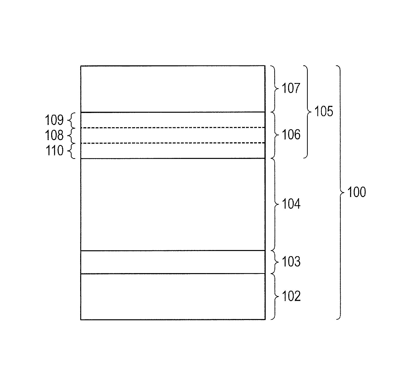
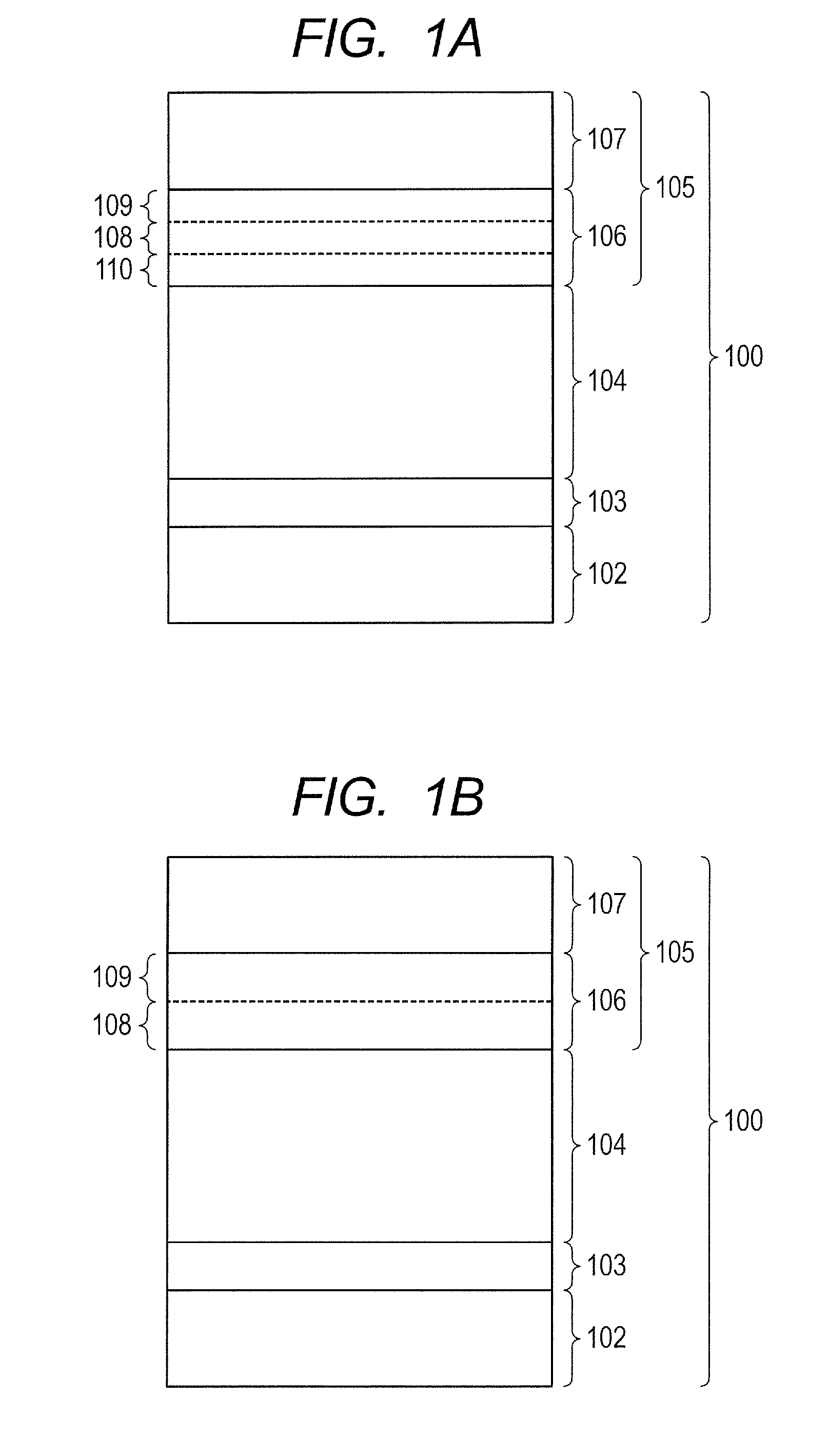
[0312]Layers illustrated in FIG. 1A and FIG. 1B were formed on the conductive substrates (substrates) 7112 which were made from aluminum and had a cylindrical shape with a diameter of 84 mm, a length of 381 mm and a thickness of 3 mm, with the use of the apparatus 7000 for forming a deposition film as illustrated in FIG. 7, on conditions shown in Table 1, and a cylindrical electrophotographic photosensitive member to be negatively electrified (a-Si photosensitive member) was manufactured.

[0313]The change region 106 was formed in the following way.

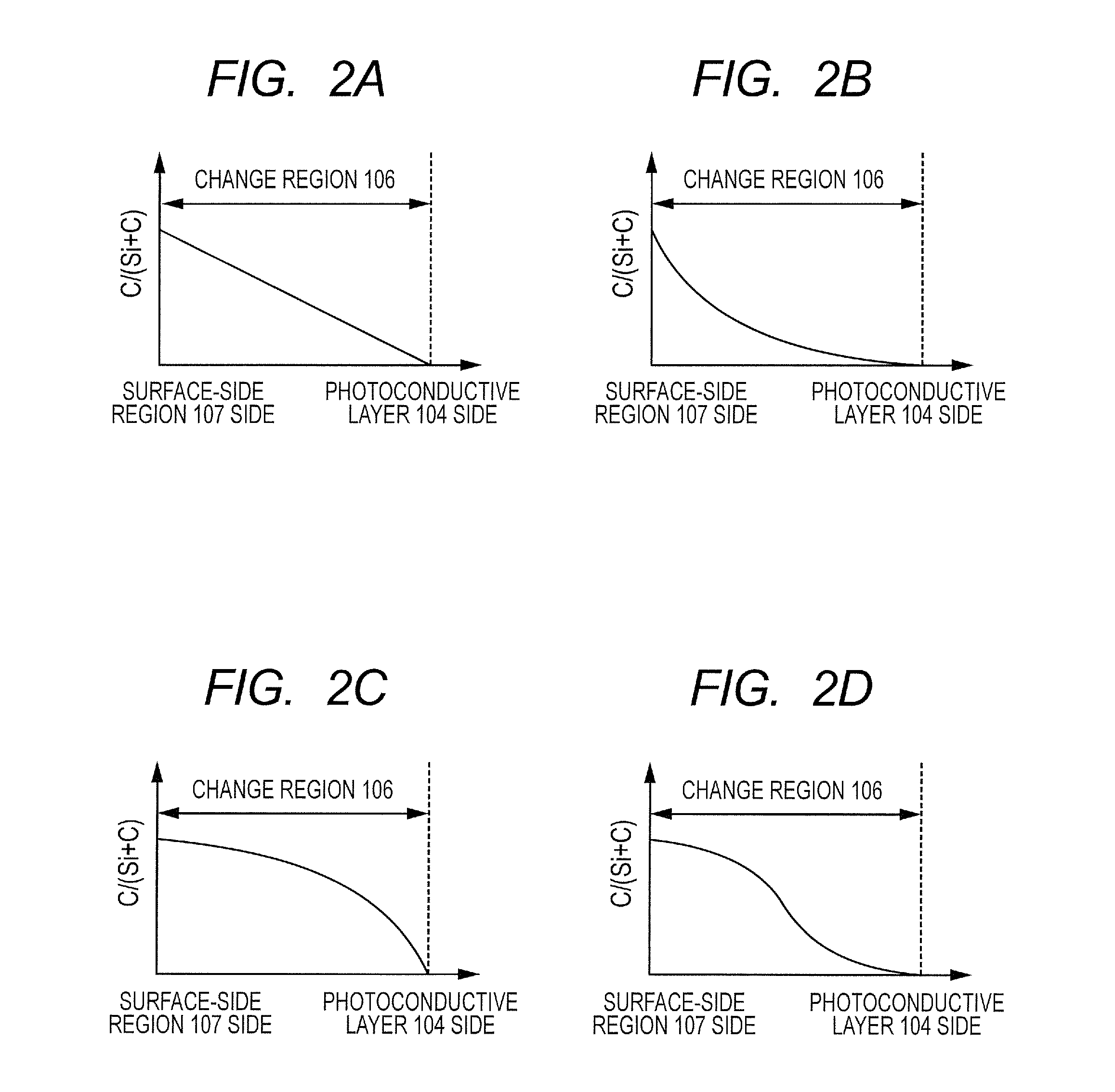
[0314]As shown in Table 1, a flow rate of SiH4 which was introduced into the reaction vessel 7110 was continuously changed from 100 [mL / min (normal)] to 90 [mL / min (normal), from 90 [mL / min (normal) to 75 [mL / min (normal)], and from 75 [mL / min (normal)] to 15 [mL / min (normal)].

[0315]At the same time, a flow rate of CH4 which was introduced into the reaction vessel 7110 was continuously changed from 25 [mL / min (normal)] to 55 [mL / min (normal...

example 2

[0340]An a-Si photosensitive member was manufactured with similar procedures to those in Example 1, except that conditions shown in Table 1 were changed to conditions shown in Table 5.

[0341]However, in the present example, the upper charge injection prohibiting portion 108 was formed in the following way.

[0342]In the conditions on which the change region 106 was formed, at the time when a flow rate of SiH4 which was introduced into the reaction vessel 7110 became 90 [mL / min (normal)] and when a flow rate of CH4 became 55 [mL / min (normal)], B2H6 was introduced into the reaction vessel 7110 for 60 seconds, and the introduction amount (flow rate) was increased from 0 ppm to 200 ppm with respect to SiH4. After that, a deposition film was formed while a flow rate of B2H6 was maintained at 200 ppm with respect to SiH4. After that, in the conditions on which the change region 106 was formed, at the time when the flow rate of SiH4 which was introduced into the reaction vessel 7110 became 75...

example 3

[0352]An a-Si photosensitive member was manufactured with similar procedures to those in Example 1, except that conditions shown in Table 1 were changed to conditions shown in Table 6.

[0353]However, in the present example, the upper charge injection prohibiting portion 108 was formed in the following way.

[0354]In the conditions on which the change region 106 was formed, at the time when a flow rate of SiH4 which was introduced into the reaction vessel 7110 became 90 [mL / min (normal)] and when a flow rate of CH4 became 55 [mL / min (normal)], B2H6 was introduced into the reaction vessel 7110 for 60 seconds, and the introduction amount (flow rate) was increased from 0 ppm to 200 ppm with respect to SiH4. After that, a deposition film was formed while a flow rate of B2H6 was maintained at 200 ppm with respect to SiH4. After that, in the conditions on which the change region 106 was formed, at the time when the flow rate of SiH4 which was introduced into the reaction vessel 7110 became 75...


PUM

PropertyMeasurementUnit
thicknessaaaaaaaaaa
thicknessaaaaaaaaaa
thicknessaaaaaaaaaa

Abstract

A surface layer of the electrophotographic photosensitive member has a change region in which a ratio of the number of carbon atoms with respect to the sum of the number of silicon atoms and the number of carbon atoms gradually increases toward a surface side of the electrophotographic photosensitive member from a photoconductive layer side, wherein the change region has an upper charge injection prohibiting portion containing a Group 13 atom, and a surface-side portion which is positioned closer to the surface side of the electrophotographic photosensitive member than the upper charge injection prohibiting portion and does not contain the Group 13 atom, and the distribution of the Group 13 atom in a boundary portion between the surface-side portion and the upper charge injection prohibiting portion is precipitous.

Description

BACKGROUND OF THE INVENTION[0001]1. Field of the Invention[0002]The present invention relates to an electrophotographic photosensitive member, a method for manufacturing the same, and an electrophotographic apparatus having the electrophotographic photosensitive member.[0003]2. Description of the Related Art[0004]As one type of an electrophotographic photosensitive member (hereinafter referred to simply as “photosensitive member” as well) to be used in an electrophotographic apparatus, a photosensitive member is known which employs hydrogenated amorphous silicon as a photoconductive material (hereinafter referred to as “a-Si photosensitive member” as well).[0005]The a-Si photosensitive member is manufactured by forming a photoconductive layer which is formed from the hydrogenated amorphous silicon on a conductive substrate (hereinafter referred to simply as “substrate” as well), generally, with a film-forming method such as a plasma CVD method.[0006]Conventionally, it has been inves...

Claims


Application Information

Patent Timeline
Patent Type & Authority Patents(United States)
IPC IPC(8): G03G5/08G03G5/05G03G5/147G03G5/082G03G5/043
CPCG03G5/043G03G5/08221G03G5/0433G03G5/0525G03G5/08G03G5/08214G03G5/08235G03G5/14704
Inventor SHIRASUNA, TOSHIYASUNISHIMURA, YUU
Owner CANON KK
Why Eureka
Try Eureka