Power module package

a technology of power module and package, applied in the direction of electrical equipment, semiconductor devices, semiconductor/solid-state device details, etc., can solve the problems of reducing and affecting the production efficiency of dbc substrates. , to achieve the effect of reducing material cost and processing expense, preventing delamination, and minimizing the influence of heat generation

Inactive Publication Date: 2015-08-11
SAMSUNG ELECTRO MECHANICS CO LTD
View PDF12 Cites 0 Cited by
  • Summary
  • Abstract
  • Description
  • Claims
  • Application Information

AI Technical Summary

Benefits of technology

[0012]Further, the present invention has been made in an effort to provide a power module package capable of minimizing an influence of heat generated from a power device to a control device.
[0013]Further, the present invention has been made in an effort to provide a power module package having reduced material cost and processing expense.
[0014]Further, the present invention has been made in an effort to provide a power module package capable of preventing delamination from occurring between metal layers.

Problems solved by technology

In general, if heat is greatly generated during a power conversion process, and the generated heat is not efficiently removed, a module and a whole system may deteriorate in terms of performance and be damaged.
However, the above-described DBC substrate has advantageously excellent heat dissipation and thermal conductivity characteristics, whereas it is disadvantageously expensive in terms of a processing characteristic, and it is difficult to manufacture a large size DBC substrate in terms of a thin ceramic characteristic.
Furthermore, the above-described DBC substrate has a structure in which the copper substrates are bonded to both sides of the ceramic, which may problematically cause delamination of the copper substrate from the ceramic.

Method used


Image

  • Power module package
  • Power module package
  • Power module package

Examples


first embodiment

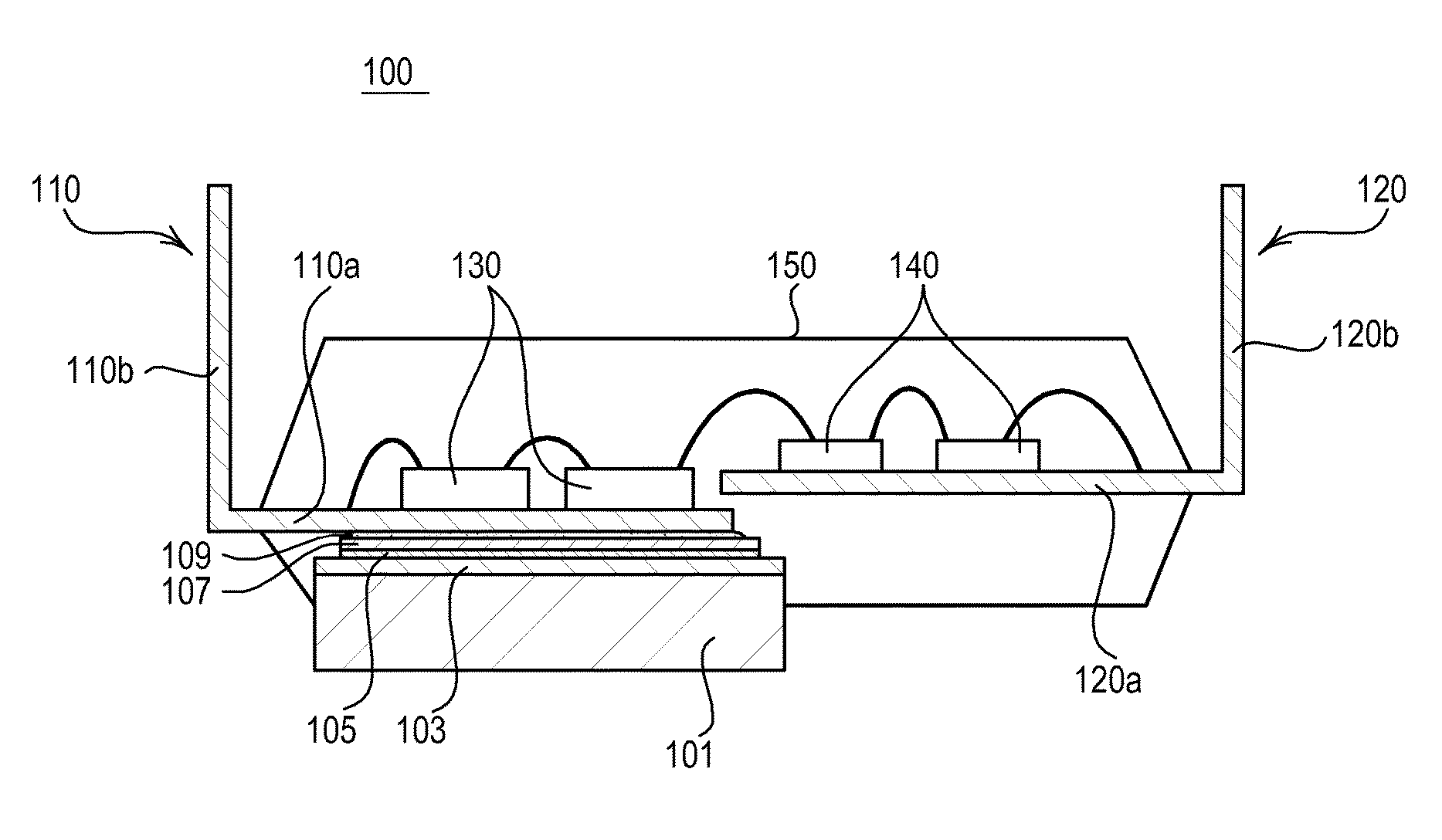
[0038]FIG. 1 is a cross-sectional view of a structure of a power module package 100 according to a first embodiment of the present invention.

[0039]Referring to FIG. 1, the power module package 100 of the present embodiment includes a substrate 101 having a ceramic layer 103 formed in one surface thereof and a circuit pattern formed on the ceramic layer 103.

[0040]Also, in the present embodiment, the power module package 100 may further include a first lead frame 110 contacting the circuit pattern and a second lead frame 120 spaced apart from the first lead frame 110.

[0041]Also, in the present embodiment, the power module package 100 may further include a first semiconductor chip 130 mounted on the first lead frame 110 and a second semiconductor chip 140 mounted on the second lead frame 120.

[0042]Although the substrate 101 may be a metal substrate in the present embodiment, the present invention is not limited thereto. For example, the substrate 101 may include a printed circuit board...

second embodiment

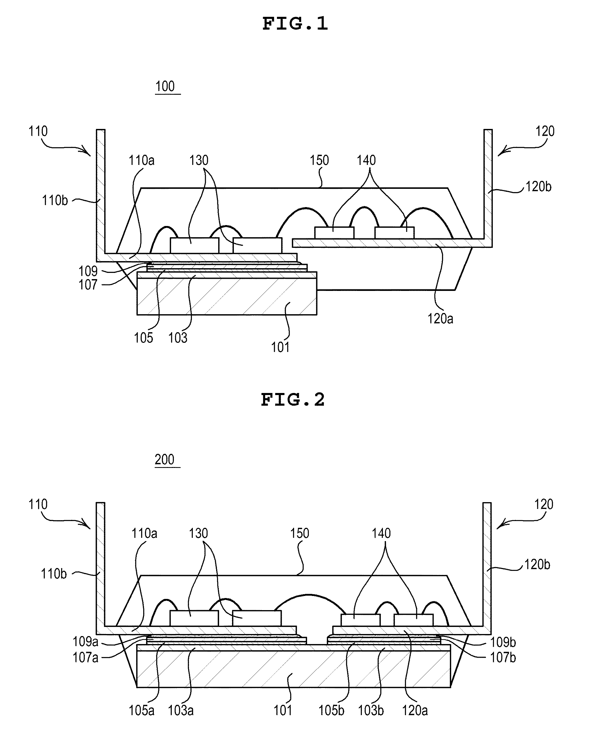
[0082]FIG. 2 is a cross-sectional view of a structure of a power module package 200 according to a second embodiment of the present invention.

[0083]Redundant descriptions between the first embodiment and the second embodiment will be omitted here, and the same reference numerals will denote the same elements therebetween.

[0084]Referring to FIG. 2, the power module package 200 according to the present embodiment has a structure in which both the first lead frame 110 and the second lead frame 120 are bonded onto the substrate 101.

[0085]That is, one side of the first lead frame 110 contacts a plating layer 107a of a circuit pattern formed on the ceramic layer 103 formed on one surface of the substrate 101, and the other side thereof protrudes from the substrate 101 toward the outside.

[0086]Likewise, one side of the second lead frame 120 contacts a plating layer 107b of a circuit pattern formed on the ceramic layer 103 formed on one surface of the substrate 101, and the other side there...

third embodiment

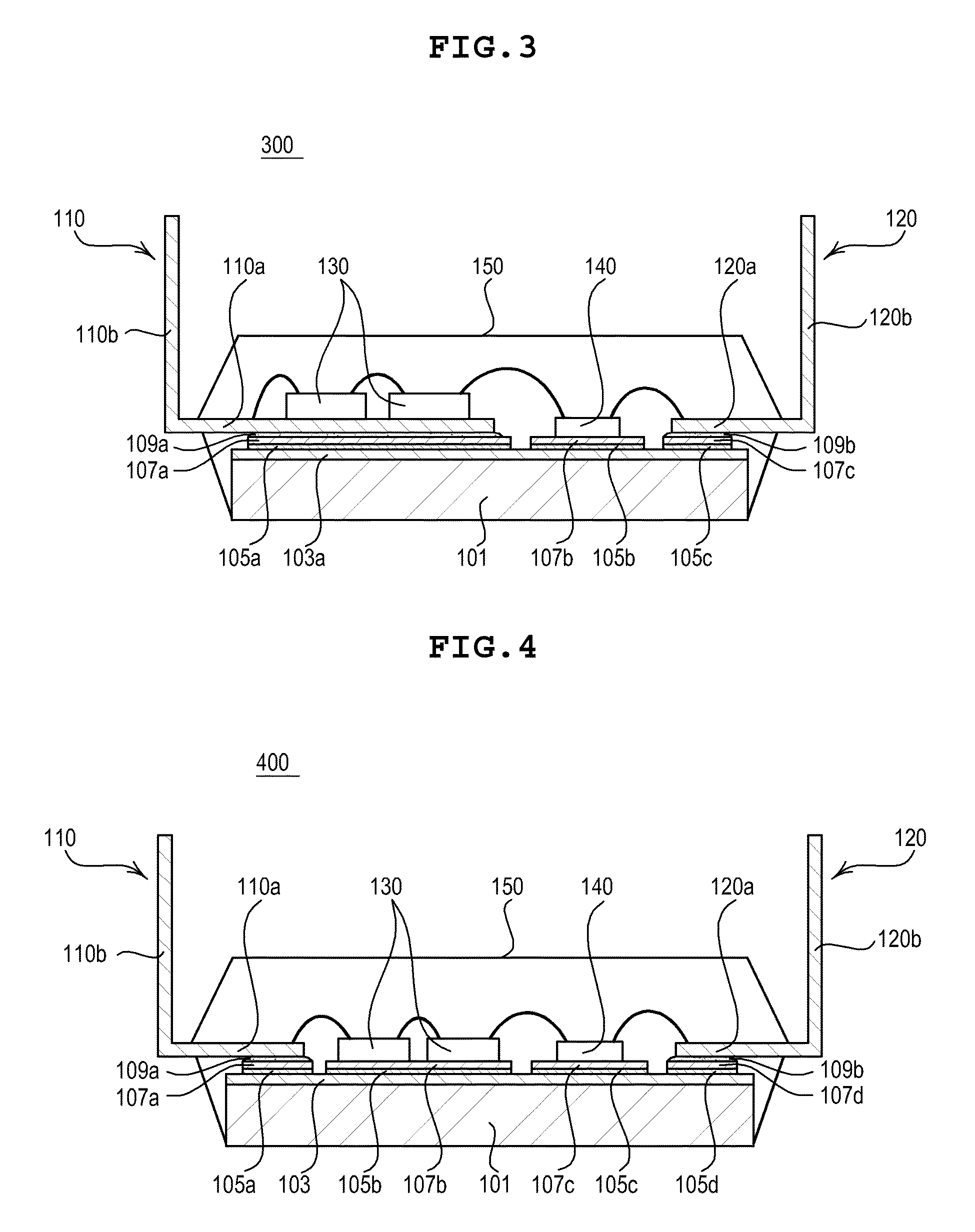
[0090]FIG. 3 is a cross-sectional view of a structure of a power module package 300 according to a second embodiment of the present invention.

[0091]Redundant descriptions between the first embodiment and the second embodiment will be omitted here, and the same reference numerals will denote the same elements therebetween.

[0092]Referring to FIG. 3, unlike the power module package 200 described according to the above-described second embodiment, the power module package 300 according to the present embodiment has a structure in which the first semiconductor chip 130 is mounted on the first lead frame 110, and the second semiconductor chip 140 is bonded onto the plating layer 107b of the circuit pattern formed on the ceramic layer 103 of the substrate 101.

[0093]The power module package 300 according to the present embodiment directly bonds the second semiconductor chip 140 that is a low power semiconductor chip for generating a relatively small amount of heat onto the plating layer 107...


PUM


Abstract

Disclosed herein is a power module package including: a substrate having a ceramic layer formed in one surface thereof; a circuit pattern formed on the ceramic layer; a first lead frame having one side contacting the circuit pattern and the other side protruding toward the outside; and a first semiconductor chip mounted on one side of the first lead frame.

Description

CROSS REFERENCE TO RELATED APPLICATION[0001]This application claims the benefit of Korean Patent Application No. 10-2011-0112335, filed on Oct. 31, 2011, entitled “Power Module Package”, which is hereby incorporated by reference in its entirety into this application.BACKGROUND OF THE INVENTION[0002]1. Technical Field[0003]The present invention relates to a power module package.[0004]2. Description of the Related Art[0005]As an amount of used energy increases worldwide, a power conversion apparatus such as an inverter for home and industry has been increasingly employed for an efficient use of energy and protection of an environment.[0006]An intelligent power module (IPM) spotlighting along with an increase in the employment of the inverter is a core parts performing functions of rectifying a DC and converting an AC and may be applied to home appliances such as a refrigerator, a washing machine, an air conditioner, etc., industrial appliances such as an industrial motor, and next gen...

Claims


Application Information

Patent Timeline
Patent Type & Authority Patents(United States)
IPC IPC(8): H01L23/495H01L23/433
CPCH01L23/4334H01L23/49531H01L23/49537H01L23/49575H01L2224/48137H01L2224/48247H01L2924/13055H01L2924/00H01L2924/13034H01L2924/00014H01L2924/13091H01L2924/1305H01L2924/181H01L2924/00012H01L23/15H01L23/34H01L23/495H01L25/16
Inventor KIM, KWANG SOOKWAK, YONG HOONYUN, SUN WOOLEE, YOUNG KIOH, KYU HWANSON, JIN SUK
Owner SAMSUNG ELECTRO MECHANICS CO LTD
Why Eureka
Try Eureka