
Alignment structures for integrated-circuit packaging

a technology of integrated circuits and alignment structures, which is applied in the direction of electrical equipment, semiconductor devices, semiconductor/solid-state device details, etc., can solve the problems of complicated assembly, high cost of ball-and-pit alignment techniques, and difficult and expensive mcm assembly, so as to facilitate the assembly of mcm, reduce symmetry, and increase elastic modulus

Active Publication Date: 2015-08-18
ORACLE INT CORP
View PDF5 Cites 4 Cited by
  • Summary
  • Abstract
  • Description
  • Claims
  • Application Information

AI Technical Summary

Benefits of technology

The patent describes a method for making a multi-layered ceramic material (MCM) by creating a positive feature with a low elastic modulus during fabrication, which makes it easier to assemble the layers of the material. The elastic modulus is then increased through thermal or optical curing. The positive feature's shape may also be designed to allow for volume movement in one or more directions during fabrication, by reducing its symmetry. The elastic modulus may be temporarily reduced during fabrication to facilitate assembly of the MCM by imparting energy to the positive feature.

Problems solved by technology

However, this ball-and-pit alignment technique can be expensive because of: the cost of silicon substrates; and the active regions on the silicon substrates that are occupied by the etch pits.
In addition, it can be difficult and expensive to assemble the MCMs because of: the difficulty of positioning the balls in the etch pits (which becomes more difficult as the size of the balls is reduced); the fact that the three components (two silicon substrates with etch pits and at least one ball) have additional degrees of freedom, which makes assembly more complicated; and the fact that the ball-and-pit alignment technique typically is not compatible with other, lower-cost substrates (such as organic or ceramic substrates).
As a consequence, the costs of MCMs that use ball-and-pit alignment can be prohibitive.

Method used


Image

  • Alignment structures for integrated-circuit packaging
  • Alignment structures for integrated-circuit packaging
  • Alignment structures for integrated-circuit packaging

Examples


Embodiment Construction

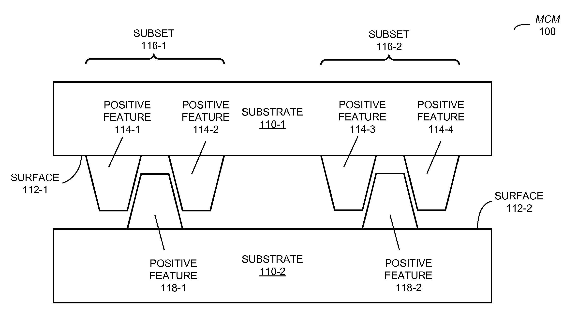
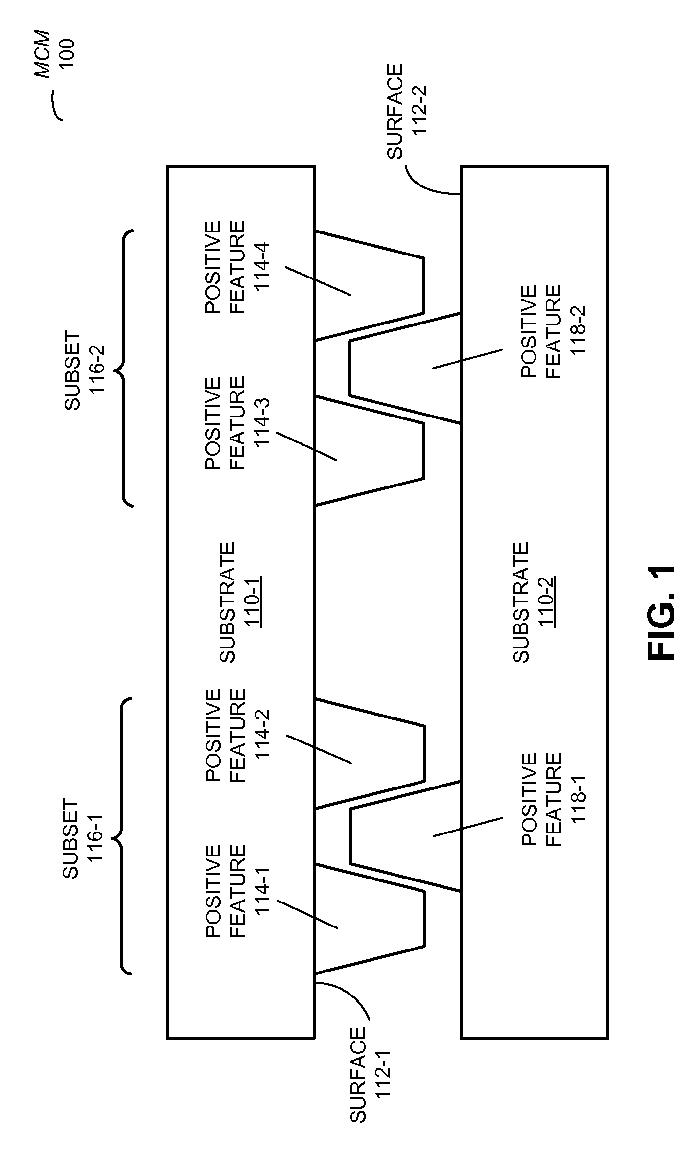
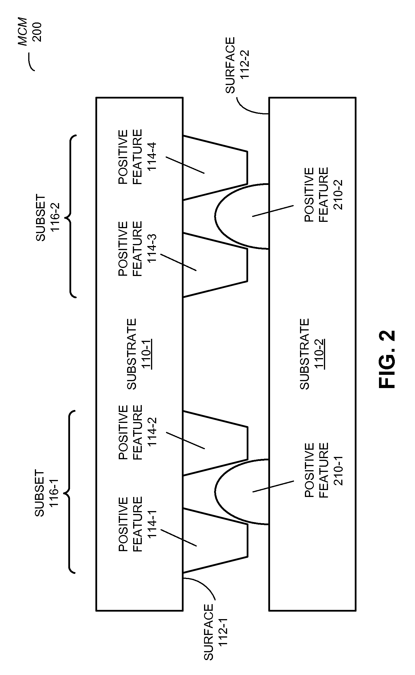
[0033]Embodiments of a multi-chip module (MCM) that includes alignment features, and a technique for fabricating the MCM are described. This MCM includes at least two substrates having facing surfaces with positive features disposed on them. Note that a given positive feature on either of the surfaces protrudes above the surface. Furthermore, the two substrates are mechanically coupled by these positive features. In particular, a given one of the positive features on one of the surfaces mates with a given subset of the positive features on the other of the surfaces. Additionally, the given subset of the positive features includes two or more of the positive features.

[0034]These alignment features in the MCM may facilitate lower-cost assembly and improved alignment of components in the MCM. In particular, by using the positive features, problems associated with assembly and alignment in the MCM may be improved or solved. For example, by using two components there are fewer degrees of...


PUM


Abstract

A multi-chip module (MCM) that includes alignment features is described. This MCM includes at least two substrates having facing surfaces with positive features disposed on them. Note that a given positive feature on either of the surfaces protrudes above the surface. Furthermore, the two substrates are mechanically coupled by these positive features. In particular, a given one of the positive features on one of the surfaces mates with a given subset of the positive features on the other of the surfaces. Additionally, the given subset of the positive features includes two or more of the positive features.

Description

BACKGROUND[0001]1. Field[0002]The present disclosure generally relates to alignment structures for integrated-circuit packaging. More specifically, the present disclosure relates to alignment structures for use in a multi-chip module (MCM) and techniques for fabricating the MCM.[0003]2. Related Art[0004]Multi-chip modules (MCMs) are being developed to facilitate proximity communication (such as capacitively coupled communication) between multiple integrated circuits (ICs) for the next generation of high-performance computers. In these MCMs, adjacent chips are often positioned face-to-face so that information can be communicated between proximity connectors (such as metal pads) on the surfaces of the facing chips.[0005]In order to enable ultrafast chip-to-chip communication speeds via capacitive coupling between the metal pads on the facing chips, these chips need to be aligned with each other on a micrometer scale. In some proposed MCMs, the alignment is obtained by using micro-sphe...

Claims


Application Information

Patent Timeline
Patent Type & Authority Patents(United States)
IPC IPC(8): H01L23/48H01L23/52H01L23/544H01L25/00H01L23/00H01L25/065
CPCH01L23/544H01L24/13H01L24/16H01L24/81H01L25/0657H01L25/50H01L2223/54426H01L2223/54473H01L2224/11013H01L2224/11015H01L2224/11848H01L2224/1301H01L2224/1319H01L2224/13021H01L2224/13023H01L2224/13078H01L2224/14179H01L2224/1601H01L2224/16145H01L2224/16147H01L2224/8112H01L2224/81191H01L2224/81193H01L2224/81897H01L2224/81948H01L2225/06513H01L2225/06531H01L2225/06565H01L2225/06593H01L2924/014H01L2924/01006H01L2924/01033H01L2924/01075H01L2924/10253H01L2924/00H01L2924/15787H01L2924/15788H01L2924/14H01L2224/0615H01L2224/131H01L2924/00014
Inventor CHOW, EUGENE M.SCHMAELZLE, PHILIPP H.
Owner ORACLE INT CORP
Learn More