Optical element, display apparatus, and method for manufacturing optical element

a technology of optical elements and display apparatuses, applied in the field of optical elements, display apparatuses, and methods for manufacturing optical elements, can solve the problems of poor adhesive properties, low degree of shape freedom, and inability to achieve weight reduction of optical elements, and achieve the effect of suppressing the deterioration of optical properties

Active Publication Date: 2015-08-25
SEIKO EPSON CORP
View PDF15 Cites 0 Cited by
  • Summary
  • Abstract
  • Description
  • Claims
  • Application Information

AI Technical Summary

Benefits of technology

[0008]An advantage of some aspects of the invention is to provide an optical element that is capable of firmly gluing a translucency member which is made of cyclo olefin polymer or cyclo olefin copolymer, to a translucency member on which a function layer is formed, while suppressing deterioration of optical properties, a display apparatus including an optical element, and a method for manufacturing an optical element.
[0011]If the optical element is configured as described above, the second translucency member that is made of cyclo olefin polymer or cyclo olefin copolymer is used, and thus there are advantages that a weight reduction can be achieved and a degree of freedom in shape is high. Furthermore, the second translucency member that is made of cyclo olefin polymer or cyclo olefin copolymer, has a low affinity to an adhesive, but the first inorganic coating layer having translucency is formed on the second translucency member, and thus the second translucency member can be firmly glued to the first translucency member. Accordingly, since it is not necessary to perform surface reforming such as light irradiation depending on a low pressure mercury lamp, irradiation with excimer ultraviolet light, plasma irradiation, and corona electric discharge, there is no possibility that transmittance is decreased due to the surface reforming.
[0014]It is preferable that the first inorganic coating layer is made of silicon oxide. Since the silicon oxide layer has a refractive index equivalent to that of the adhesive layer, it is possible to suppress a change in optical properties even in case of arranging the silicon oxide layer (the first inorganic coating layer).

Problems solved by technology

Since the prisms according to JP-A-2006-154388 and JP-A-2004-317828 are made of inorganic materials, there are problems that it is not possible to achieve a weight reduction in the optical element and a degree of freedom in shape is low.
However, since a surface of the translucency member which is made of cyclo olefin polymer or cyclo olefin copolymer is inactive, adhesive properties are poor.
However, if the surface treatment is performed, the transmittance is decreased due to transmutation, and thus it is not suitable for manufacturing the optical element.

Method used


Image

  • Optical element, display apparatus, and method for manufacturing optical element
  • Optical element, display apparatus, and method for manufacturing optical element
  • Optical element, display apparatus, and method for manufacturing optical element

Examples


embodiment 1

Configuration of Optical Element

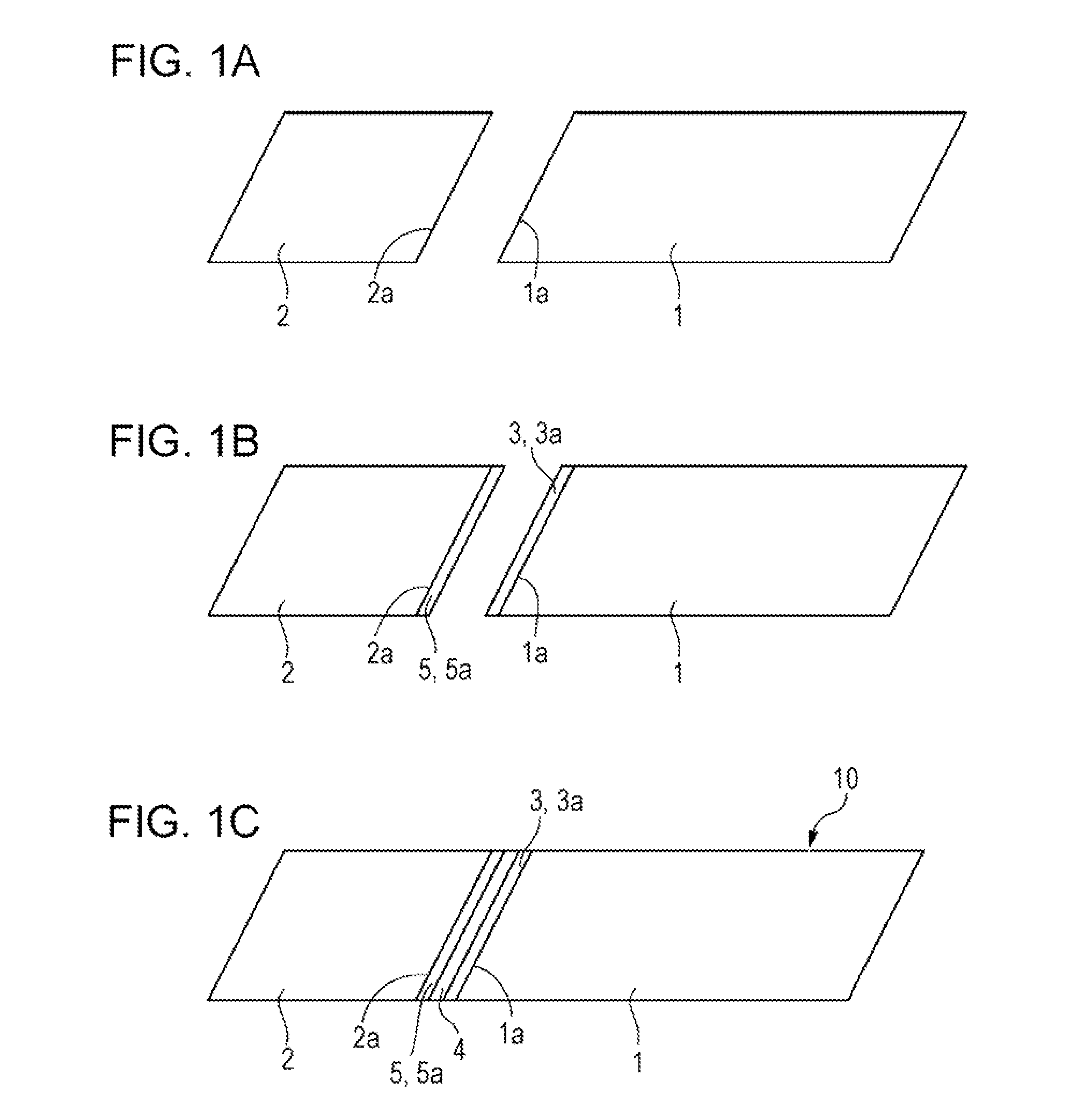
[0028]FIGS. 1A to 1C are diagrams illustrating an optical element according to Embodiment 1 of the invention. FIG. 1A is a diagram illustrating translucency members which are used in the optical element, FIG. 1B is a diagram illustrating a state before bonding the two translucency members, and FIG. 1C is a diagram illustrating the state as an optical element by bonding the two translucency members.

[0029]An optical element 10 which is shown in FIG. 1C, has a structure that two translucency members are bonded by an adhesive layer 4 interposing a functional layer 3 therebetween. More specifically, the optical element 10 includes a first translucency member 1, a second translucency member 2 that is made of cyclo olefin polymer or cyclo olefin copolymer, the functional layer 3 that is formed between the first translucency member 1 and the second translucency member 2, and the adhesive layer 4 having translucency that is formed between the functional layer ...

embodiment

Main Effect of Embodiment

[0043]As described above, if the optical element 10 is configured according to the optical element 10 of the embodiment and the method for manufacturing thereof, the second translucency member 2 that is made of cyclo olefin polymer or cyclo olefin copolymer is used, and thus there are advantages that a weight reduction can be achieved and a degree of freedom in shape is high.

[0044]Furthermore, the second translucency member 2 that is made of cyclo olefin polymer or cyclo olefin copolymer, has a low affinity to the adhesive, but the inorganic coating layer 5 having translucency is formed on the second translucency member 2, and thus the second translucency member 2 can be firmly glued to the first translucency member 1. Accordingly, since it is not necessary to perform surface reforming such as light irradiation depending on the low pressure mercury lamp, irradiation with the excimer ultraviolet light, plasma irradiation, and corona electric discharge, there ...

embodiment 2

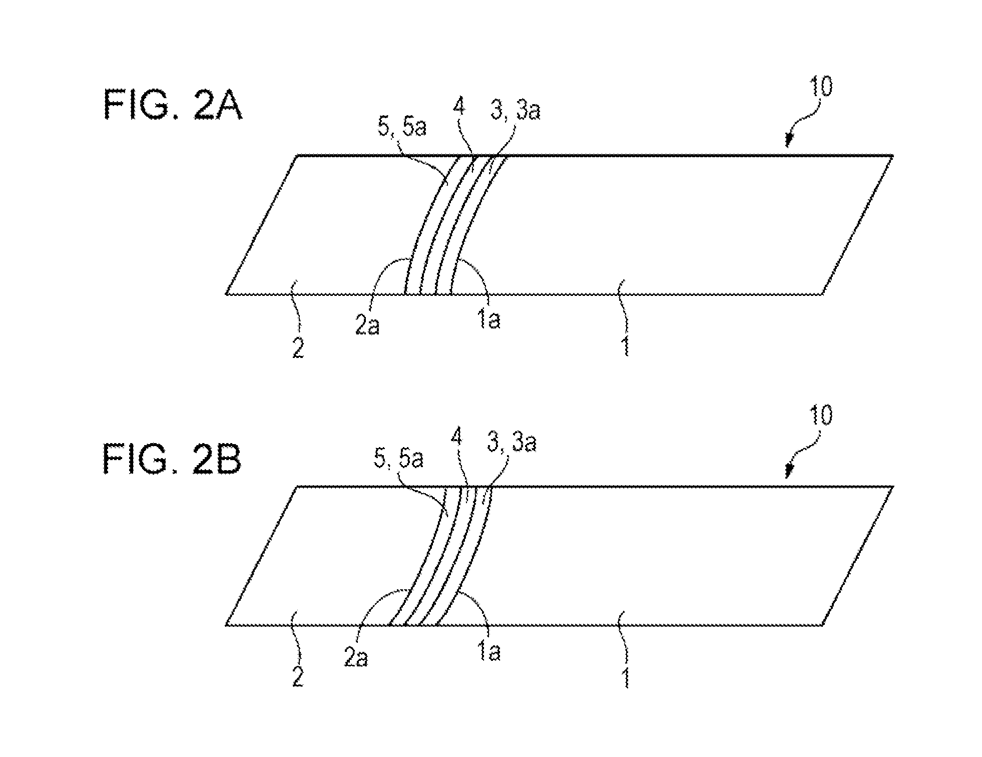
[0049]FIGS. 4A to 4D are diagrams illustrating an optical element according to Embodiment 2 of the invention. FIG. 4A is a diagram illustrating the translucency member used in the optical element, FIG. 4B is a diagram illustrating the state of arranging the coating layer on the second translucency member side, FIG. 4C is a diagram illustrating the state of arranging the coating layer on the first translucency member side, and FIG. 4D is a diagram illustrating the state of making as the optical element by bonding the two translucency members.

[0050]The optical element 10 shown in FIG. 4D, includes the second translucency member 2 that is made of cyclo olefin polymer or cyclo olefin copolymer, the functional layer 3 that is formed between the first translucency member 1 and the second translucency member 2, the adhesive layer 4 having translucency that is formed between the functional layer 3 and the second translucency member 2, in the same manner as Embodiment 1. In the embodiment, t...


PUM


Abstract

A method for manufacturing an optical element includes forming a functional layer (half mirror layer) on a first face of a first translucency member that is made of cyclo olefin polymer or cyclo olefin copolymer, and forming an inorganic coating layer having translucency (silicon oxide layer) on a second face of a second translucency member that is made of cyclo olefin polymer or cyclo olefin copolymer. The method for manufacturing an optical element further includes bonding the first face side of the first translucency member to the second face side of the second translucency member by an adhesive layer.

Description

BACKGROUND[0001]1. Technical Field[0002]The present invention relates to an optical element including a functional layer between a first translucency member and a second translucency member, a display apparatus including an optical element, and a method for manufacturing an optical element.[0003]2. Related Art[0004]At the time of manufacturing an optical element including a functional layer between two translucency members, a method for bonding the two translucency members by an adhesive after forming the functional layer on one of the two translucency members, is adopted. For example, when a dichroic mirror is manufactured, after forming the functional layer on an inclined face of a first prism, the inclined face of a second prism is bonded to the inclined face of the first prism by the adhesive (see JPA-2006-154388 and JP-A-2004-317828). Furthermore, in JPA-2006-154388, forming a silicon oxide layer on the inclined face of the second prism, and thereby improving a wavefront aberra...

Claims


Application Information

Patent Timeline
Patent Type & Authority Patents(United States)
IPC IPC(8): G02B27/01G02B27/14G02B27/10
CPCG02B27/144G02B27/1073G02B27/017G02B2027/0178Y10T428/24521Y10T428/31938
Inventor USHIYAMA, KAZUHIRO
Owner SEIKO EPSON CORP
Why Eureka
Try Eureka