Demodulation pixel with backside illumination and charge barrier

a backside illumination and charge barrier technology, applied in the direction of photoelectric discharge tubes, electrical apparatus, electric discharge tubes, etc., can solve the problems of limited use of micro-lenses, near-infra red (nir) photons penetrate deeper in the substrate, etc., and achieve the effect of increasing quantum efficiency

Active Publication Date: 2015-08-25
AMS SENSORS SINGAPORE PTE LTD
View PDF22 Cites 38 Cited by
  • Summary
  • Abstract
  • Description
  • Claims
  • Application Information

AI Technical Summary

Benefits of technology

[0019]The invention disclosed herein provides an enhancement of prior-art demodulation pixels in terms of sensitivity and depending on the implementation, in terms of speed.
[0020]The sensitivity is increased by the fill factor, which can reach up to 100%, and the capability of capturing photo-generated charges deep in the silicon, hence increasing quantum efficiency (QE) for long wavelengths.

Problems solved by technology

One of the main challenges of 3D TOF pixels is to collect and store quickly as many photo-generated electrons as possible in the storage nodes.
A common issue is that near-infra red (NIR) photons penetrate deeper in the substrate compared to photons in the visible spectra.
This creates the challenge to bring the photons impinging on the pixel through all the stack layers into the photo-sensitive area.
However, the use of micro-lenses has limitations as soon as the layer stack gets too big in relation to the pixel pitch.

Method used


Image

  • Demodulation pixel with backside illumination and charge barrier
  • Demodulation pixel with backside illumination and charge barrier
  • Demodulation pixel with backside illumination and charge barrier

Examples


Embodiment Construction

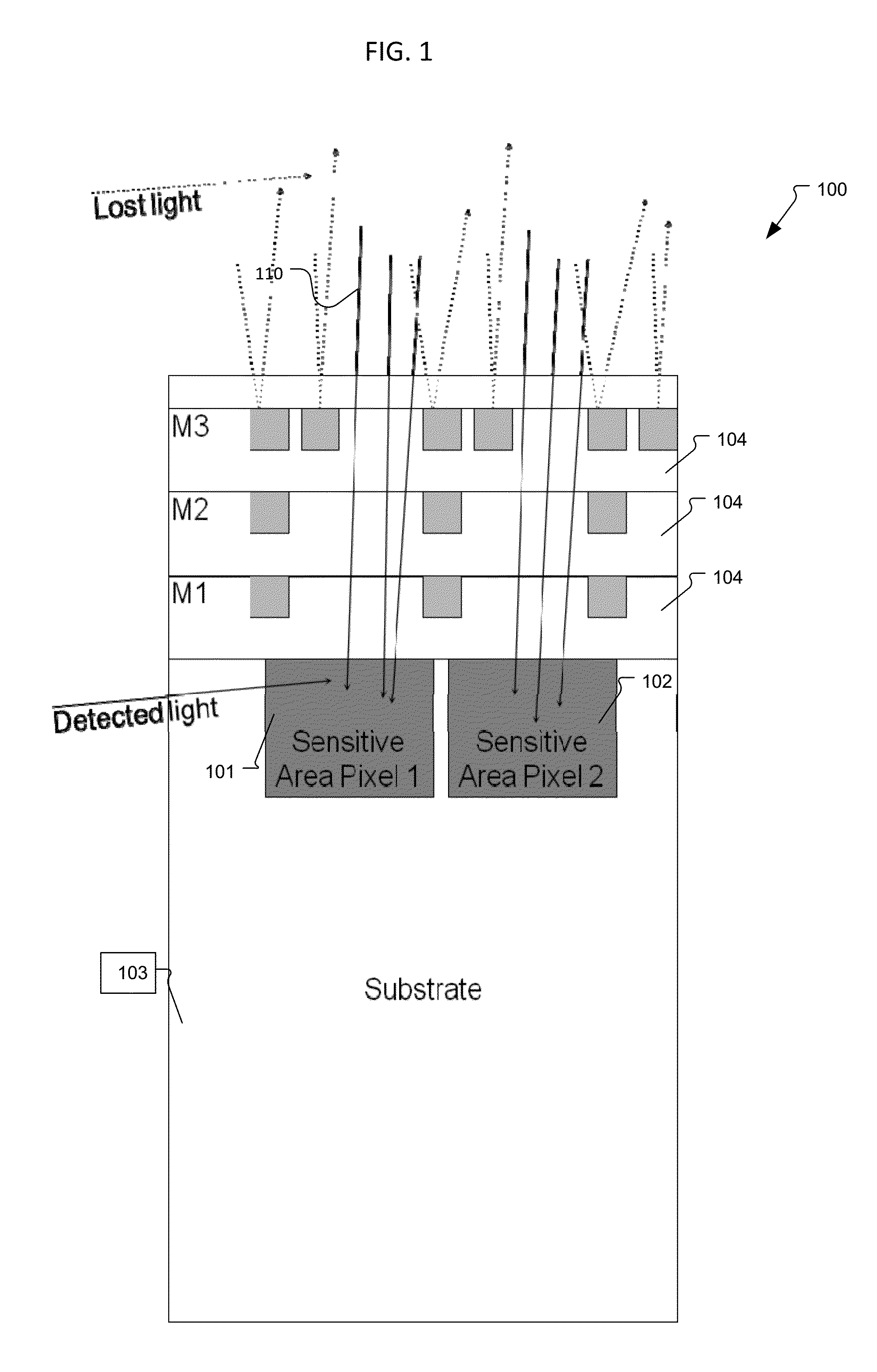
[0032]A drawback of state-of-the-art TOF pixels is that the pixels 101, 102 suffer from quite a low fill factor. This is mainly due to the electrical circuits required in the TOF pixel. A front side illuminated (FSI) sensor 100 with such a low fill factor is illustrated in FIG. 1. The metal layers 104 cover part of the pixel area and hinder the arriving photons 110 to reach the sensitive areas 101, 102.

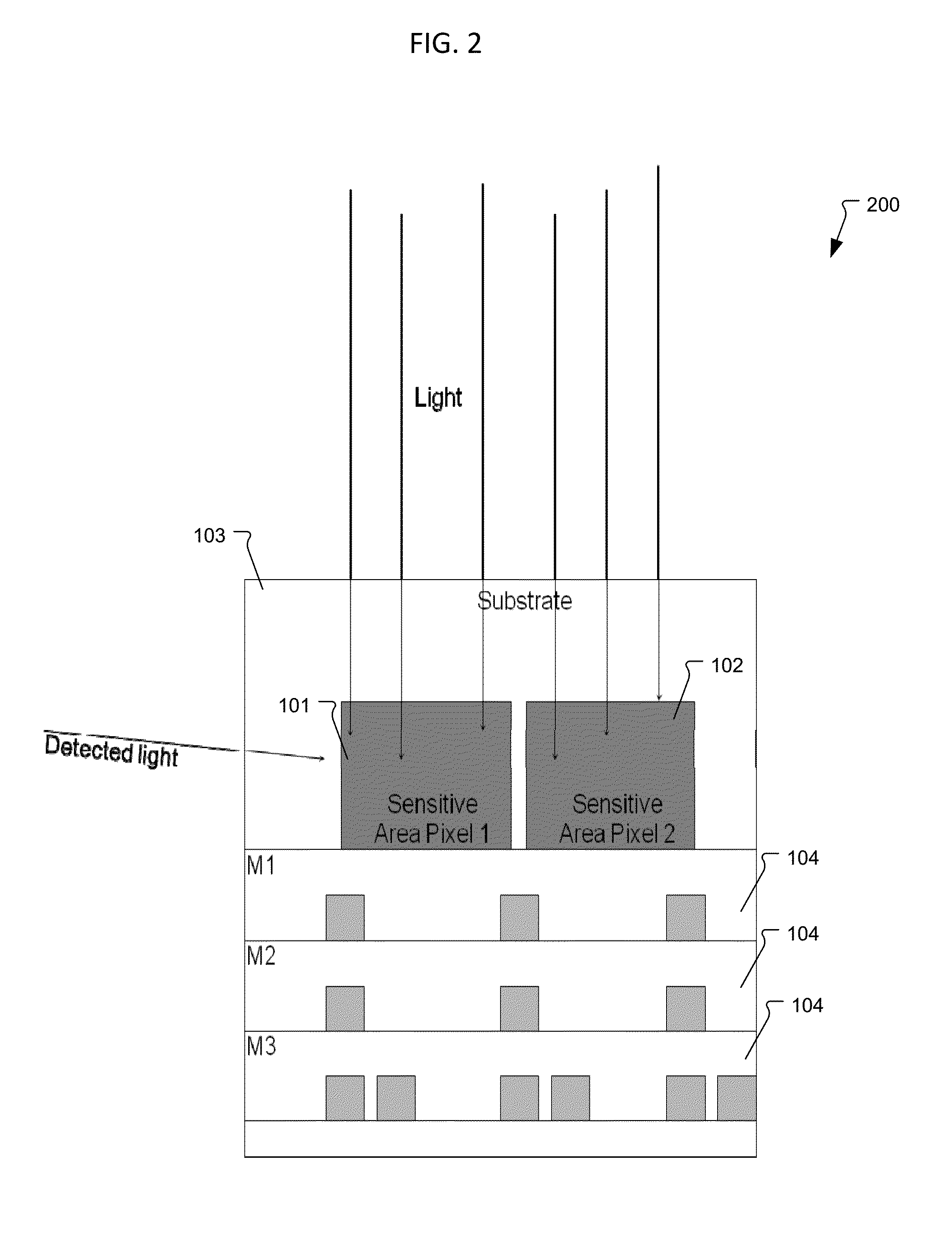
[0033]FIG. 2 illustrates a back side illuminated (BSI) senor 200, which has increased fill factor since the effective are of the sensitive areas 101 and 102 is larger.

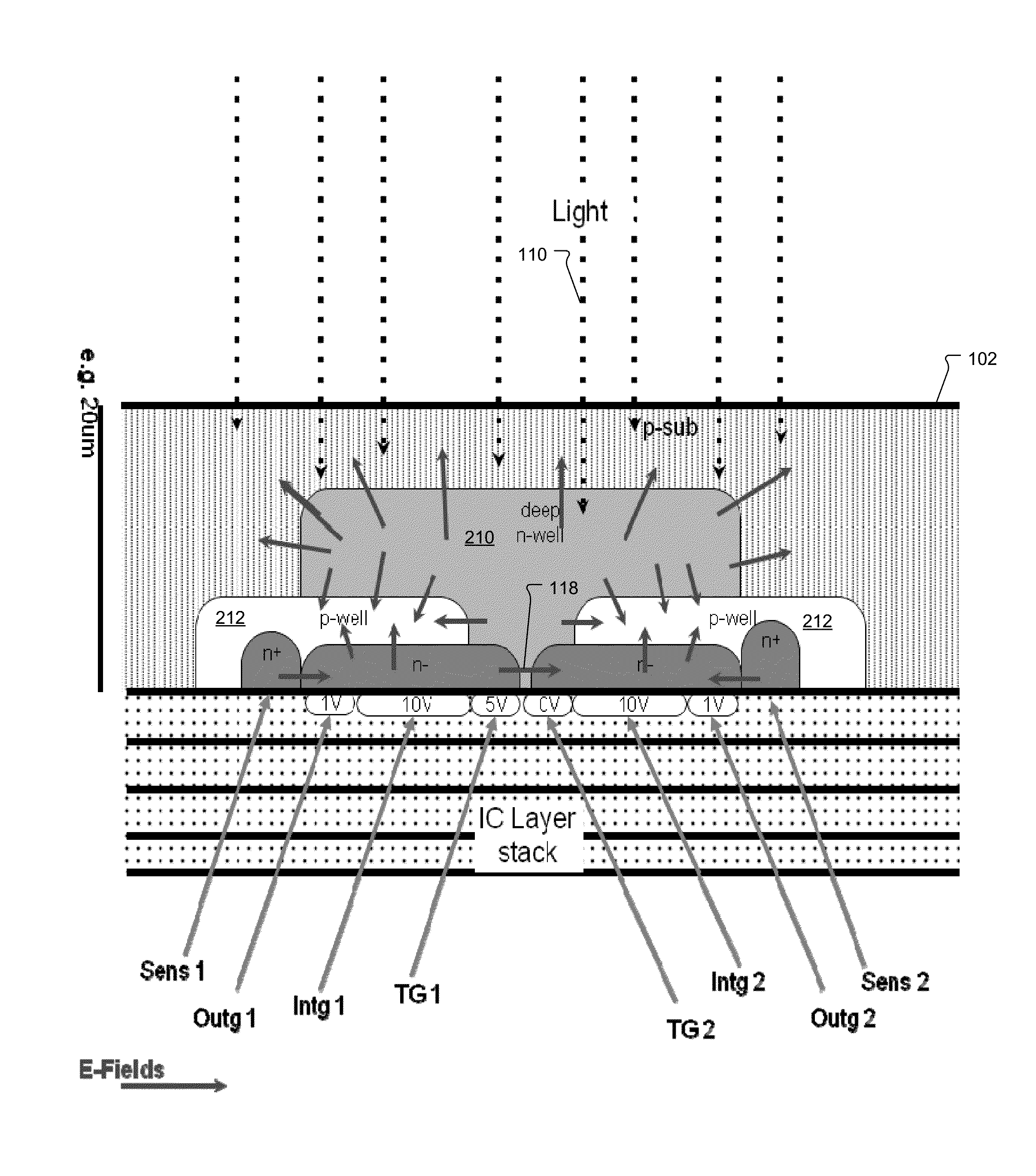
[0034]A second drawback of 3D TOF pixel is the aforementioned near-infra red (NIR) photon penetration in the silicon. While the demodulation generally takes place close to the front side of the silicon surface, the electrons need to be first of all detected deeply in the silicon and secondly transferred quickly to the corresponding storage node.

[0035]In FSI imager sensors, the depletion region usually reaches depths into...


PUM


Abstract

A high-speed, high-sensitivity demodulation sensor usable for e.g. time-of-flight application uses a back side illuminated (BSI) image sensor chip, in which the photo-generated charges are first transferred to a demodulation area, from which the charges are then sampled and stored on at least one specific storage node. The storage node is electrically isolated from the sensitive area. Such a pixel might find its use specifically in 3D time-of-flight imaging given its improvements in sensitivity because the presented invention allows to design pixel with up to 100% fill factor and enables charge detection even if the charge generation by the photon occurs deep in the silicon substrate.

Description

RELATED APPLICATIONS[0001]This application claims the benefit under 35 USC 119(e) of U.S. Provisional Application No. 61 / 228,198 filed on Jul. 24, 2009, which is incorporated herein by reference in its entirety.BACKGROUND OF THE INVENTION[0002]Three Dimensional (3D) time-of-flight (TOF) cameras are capable of getting range information for all pixels of the TOF detector in real-time. TOF cameras typically include a light source for illuminating the scene with modulated light, usually light emitting diodes (LEDs) or laser diodes, an optical lens system to form an image of the scene on an image sensor, and the image sensor comprising an array of high-speed demodulation pixels.[0003]Other TOF approaches might use single photon avalanche diodes (SPAD) to detect the time of flight. SPADs measure the travel time of the light from the emitter to the object and back to the camera directly, whereas demodulation pixels are measuring the back-reflected phase information or correlation informati...

Claims


Application Information

Patent Timeline
Patent Type & Authority Patents(United States)
IPC IPC(8): H01L27/00H01L31/00H01J40/14H01L27/146
CPCH01L27/14609H01L27/1463H01L27/14603H01L27/1461H01L27/1464
Inventor OGGIER, THIERRYLEHMANN, MICHAEL
Owner AMS SENSORS SINGAPORE PTE LTD
Why Eureka
Try Eureka