
Output circuit, temperature switch IC, and battery pack
a technology of output circuit and temperature switch, applied in the field of output circuit, can solve problems such as large area of output circuit, and achieve the effect of reducing area and restricting unstable outputs
- Summary
- Abstract
- Description
- Claims
- Application Information
AI Technical Summary
Benefits of technology
Problems solved by technology
Method used
Image

Examples
Embodiment Construction
[0022]Embodiments of the present invention will be described below with reference to the accompanying drawings.
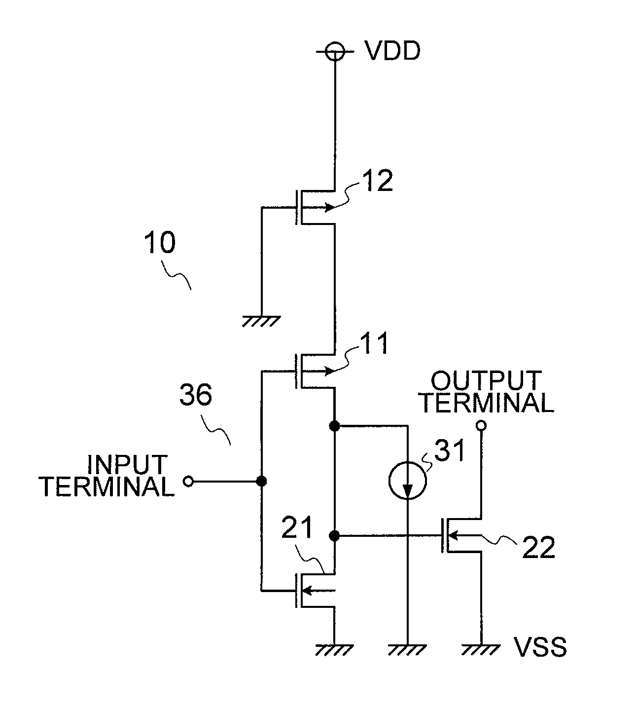
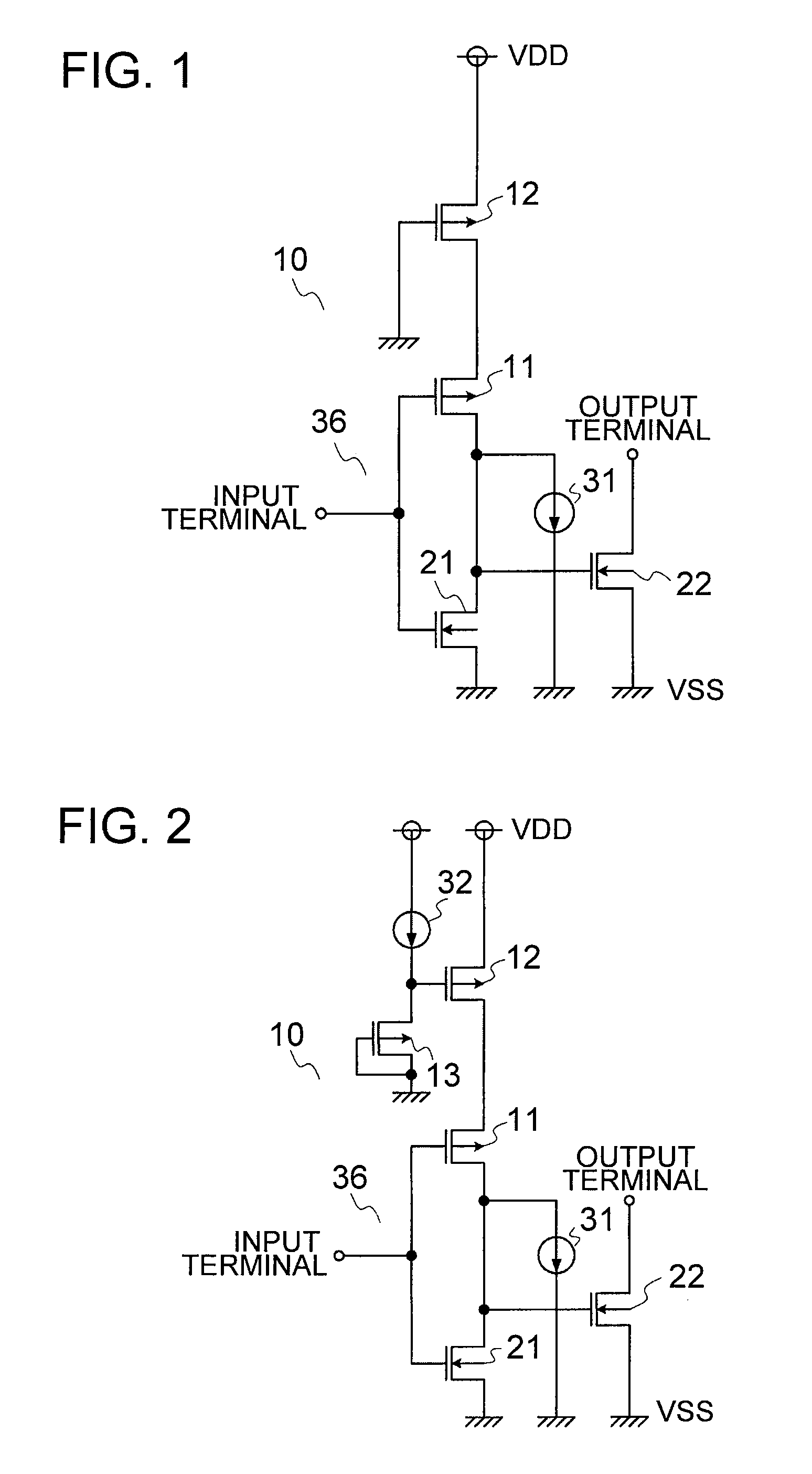
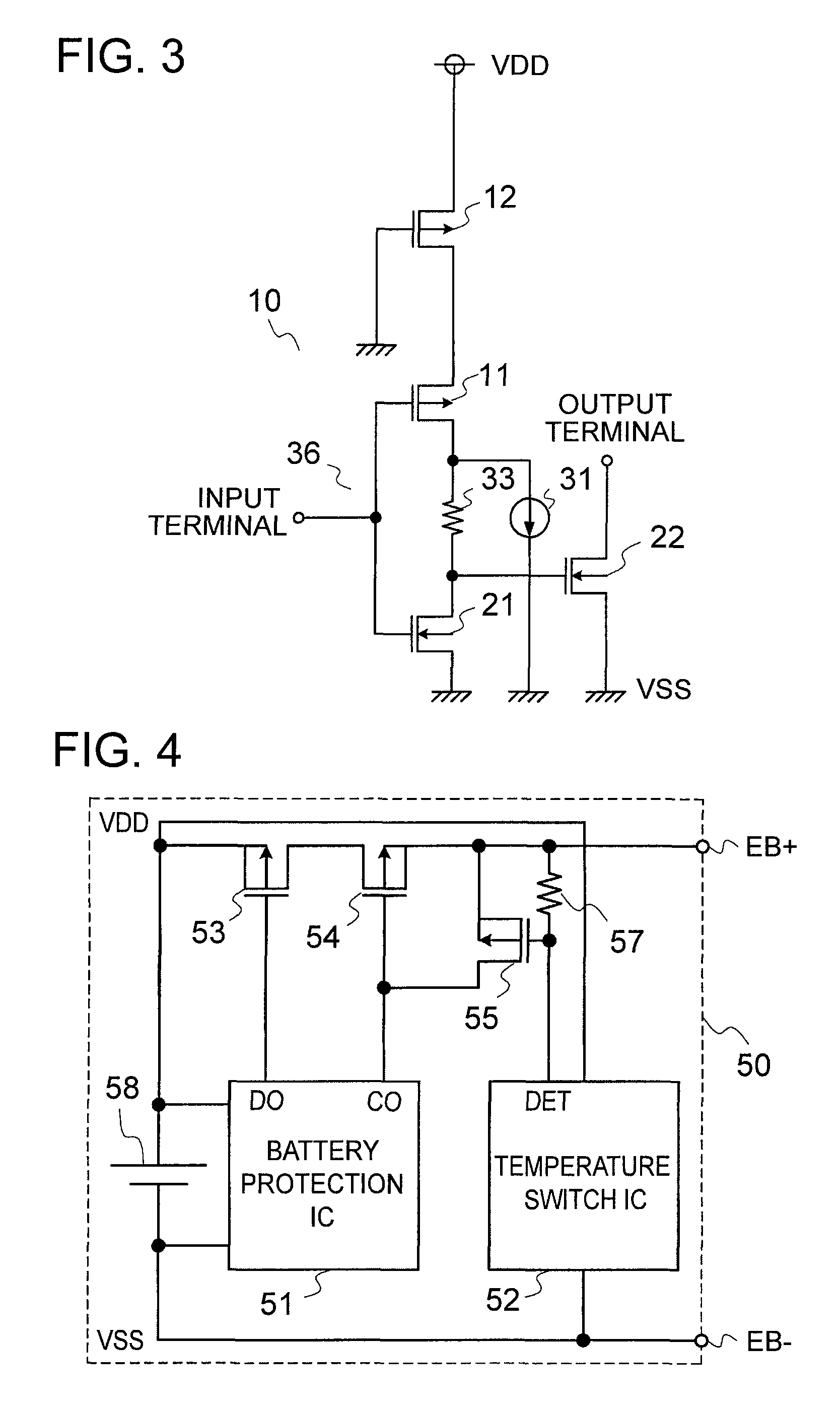
[0023]FIG. 1 is a circuit diagram illustrating an output circuit according to an embodiment of the present invention.
[0024]An output circuit 10 has PMOS transistors 11 and 12, NMOS transistors 21 and 22, and a current source 31.
[0025]The PMOS transistor 11 has the gate thereof connected to the input terminal of the output circuit 10, the source thereof connected to the drain of the PMOS transistor 12, and the drain thereof connected to the gate of the NMOS transistor 22. The NMOS transistor 21 has the gate thereof connected to the input terminal of the output circuit, the source thereof connected to an earth terminal (a power supply terminal at an earth voltage side), and the drain thereof connected to the gate of the NMOS transistor 22. The PMOS transistor 12 has the gate thereof connected to the earth terminal and the source thereof connected to a supply terminal (the pow...
PUM
 Abstract
Description
Claims
Application Information