
Methods for fabrication of parts from bulk low-cost interface-defined nanolaminated materials

a technology of interface-defined nanolaminates and parts, applied in the field of nanolaminates, can solve the problems of reducing the efficiency of laminated materials, etc., to achieve novel, highly desirable properties, and maximize another property of nanolaminates.

Inactive Publication Date: 2015-09-01
THE UNITED STATES OF AMERICA AS REPRESETNED BY THE SEC OF THE AIR FORCE
View PDF91 Cites 2 Cited by
  • Summary
  • Abstract
  • Description
  • Claims
  • Application Information

AI Technical Summary

Benefits of technology

This patent describes a new type of material made up of many layers that are arranged in a way that each layer is different. These materials are made from powders that are ultimately formed into a solid shape. The unique design of these materials makes them have very different properties and structures, which makes them highly desirable. The materials' properties are controlled mainly by the engineered interfaces between the layers, which means the materials used to make the layers don't need to control how energy flows through the material. This allows for the layers to be chosen that will maximize the material's other properties.

Problems solved by technology

Though each barrier may be small, the sheer number of them and their sequential nature ultimately overwhelms the incoming energy or matter and slows down its rate of flow through the material to a small fraction of the original value.
However, even when the scattering coefficient is small, the sheer number of barriers gives tremendous power to the approach of laminated materials.
Presently, despite their attractive properties, conventional nanolaminates have some very serious drawbacks from the point of view of industrial and commercial applications.
With the exception of some high tech uses that require very small samples such as reading heads in magnetic storage, nanolaminates are prohibitively expensive for most industrial applications.
A few industrial methods to make bulk nanolayered materials exist, such as the manufacture of nanolayered materials comprising exfoliated graphite, vermiculate, and mica-type thermal insulation, which produces a single-component i.e. single composition material with incoherent interfaces; however, the continuity of individual layers in such materials is limited by the size of flakes, which is normally below 1 cm.
A multiple-extrusion step approach has also been utilized in the electronics industry to make nanometer-thick layers in Channeltron photo-multiplier tubes and superconductor wires; however, neither of these methods is applicable to fabrication of bulk quantities of two-dimensional nanolayered materials.
These manufacturing methods are generally very slow (1 to 5 μm / min) and require expensive equipment, very clean conditions, and high vacuum, as the nanolaminates are essentially built-up one atom at a time.
However, the sample size of materials made in this way is limited, and the cost to make commercial products with these techniques is prohibitive, making scale-up of these methods to industrially meaningful proportions unrealistic.
Manufacture of nanolaminates comprising shapes with a high aspect ratio such as tubes or rods presents additional challenges.
Manufacturing a high aspect ratio, nanolaminate part with a sufficient number of layers is thus extremely expensive, time-consuming, and impractical using conventional methods.
In addition, while laminates and nanolaminates with coherent interfaces possess many useful properties such as high conductivity, enhanced bonding, and minimum distortion across the interface, coherency is frequently undesirable as materials with coherent interfaces are usually quite brittle and have low thermal stability.
Thus, to inhibit the propagation of energy, such as thermal energy or crack propagation perpendicular to the interfaces, it is desirable to have an incoherent interface between the layers of the laminate because coherent interfaces do not effectively scatter the energy perpendicular to them.
Furthermore, because coherency at the interfaces leads to poor thermal stability, most superlattices are unstable even at room temperatures and quickly interdiffuse, losing their nanoscopic properties at or just above ambient temperatures.

Method used


Image

  • Methods for fabrication of parts from bulk low-cost interface-defined nanolaminated materials
  • Methods for fabrication of parts from bulk low-cost interface-defined nanolaminated materials
  • Methods for fabrication of parts from bulk low-cost interface-defined nanolaminated materials

Examples


Embodiment Construction

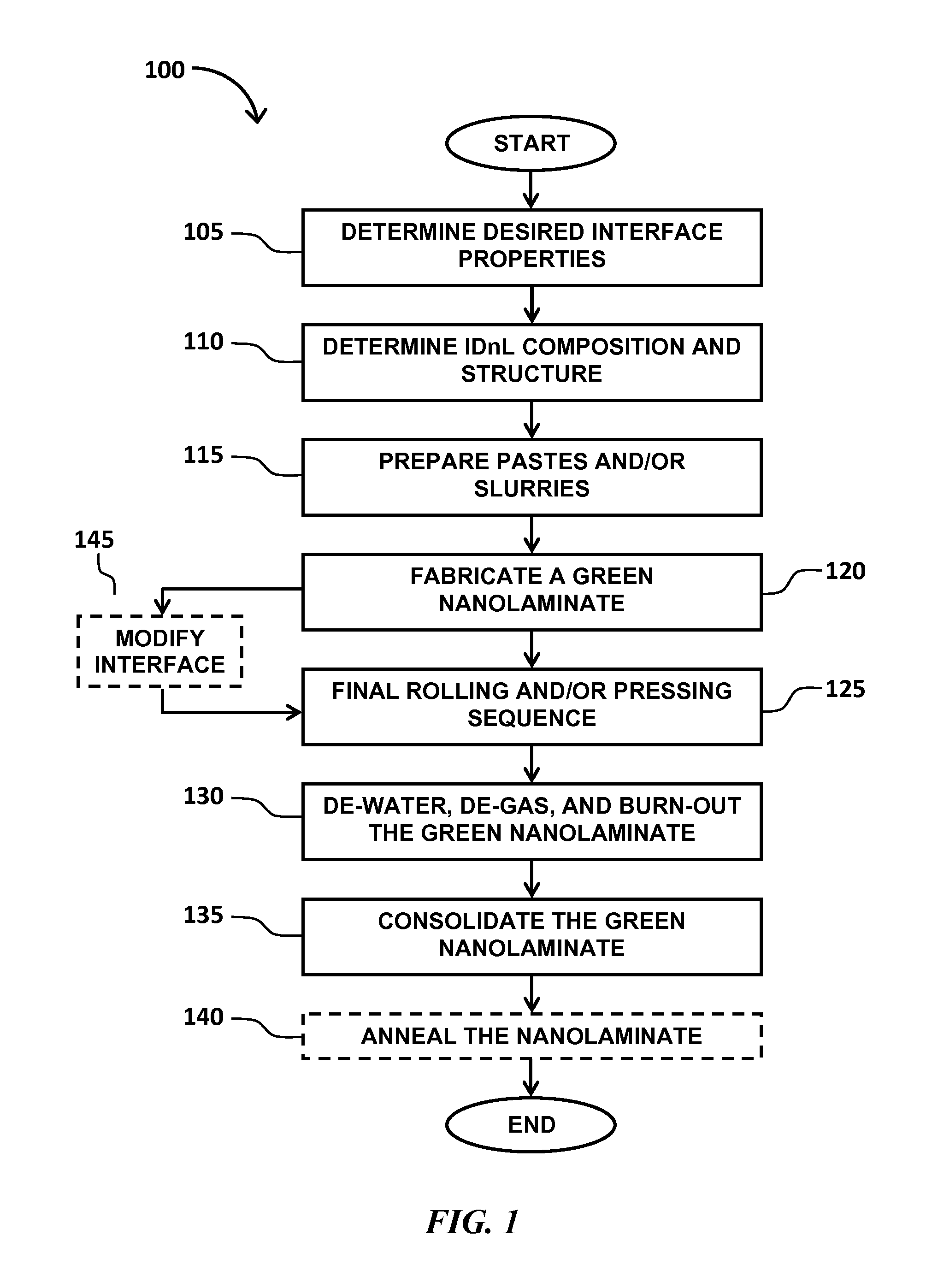
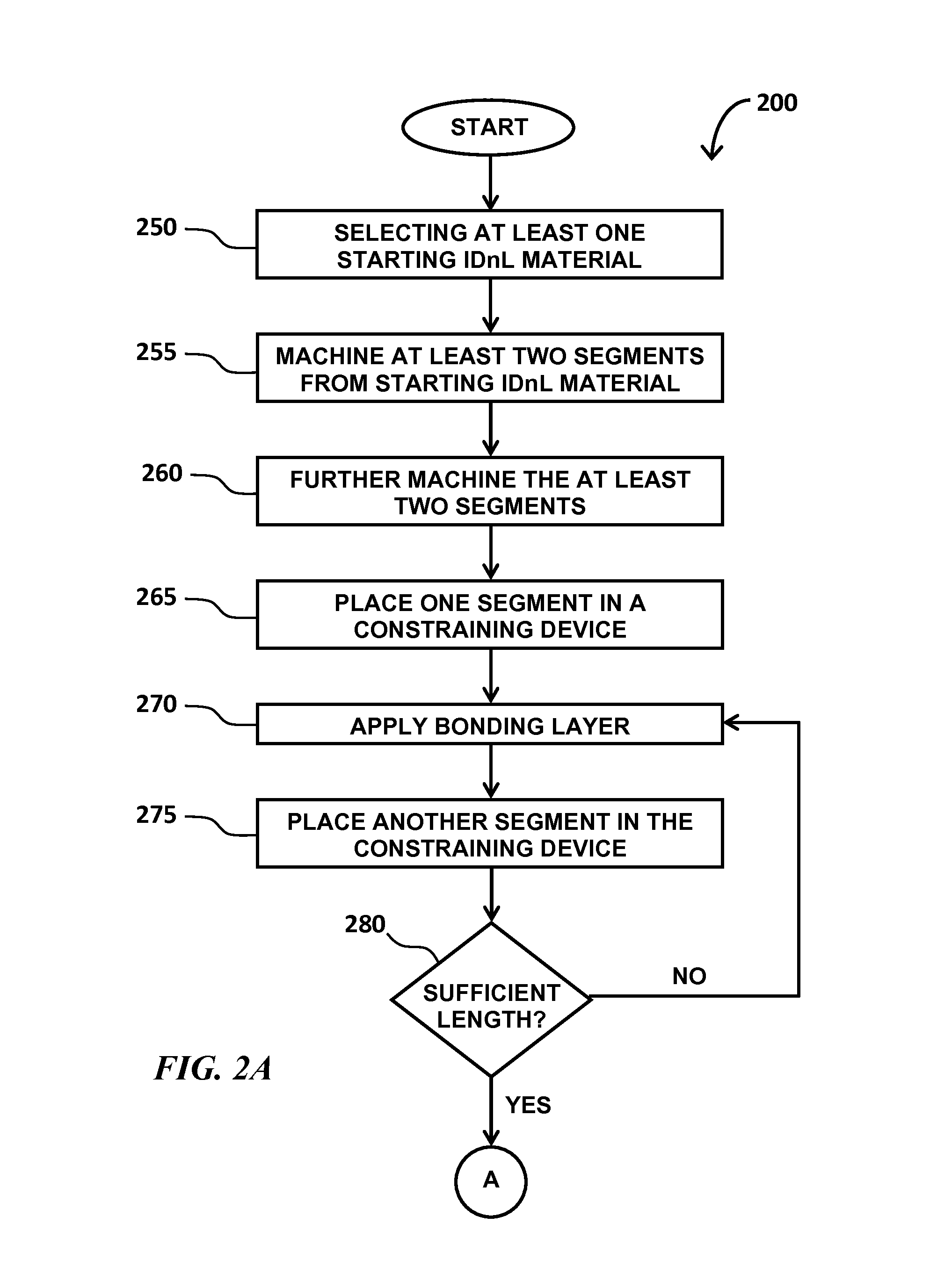
[0027]The present invention describes Interface-Defined nanoLaminate (IDnL) materials, which are novel nanolaminate materials fabricated from metals, ceramics, and other materials. The presently described IDnLs may have application in such diverse fields as fast ion conductors, magnetostrictive materials, semiconductors, hydrogen storage materials, superconductors, and environmental barrier materials and coatings. The interfaces between the layers of the IDnL materials may be designed and fabricated from many different materials. By varying the manufacturing process, the degree of atomic coherency may be varied from nearly coherent i.e. with lattice planes crossing from one material to another across the interface to completely incoherent i.e. where the lattice planes end at the interface. The present invention further includes low-cost methods to fabricate large (>0.1 square meter and preferably >1 square meter), bulk quantities of these nanolaminate materials, as well as methods f...


PUM

PropertyMeasurementUnit
thicknessaaaaaaaaaa
thicknessaaaaaaaaaa
distanceaaaaaaaaaa

Abstract

This present invention describes interface-defined nanolaminates (IDnLs), which are novel nanolaminate materials fabricated from metals and ceramics, and new methods for fabricating these IDnL materials, including new methods for manufacturing high aspect ratio parts comprising IDnL materials according to the present invention. IDnLs are fundamentally different from ordinary laminates in that their properties are defined by the interfaces between the layers rather by the properties of the bulk materials comprising the individual layers. In contrast to superlattice materials, IDnLs may be made thermally stable due to the wide selection of interface-defining materials, which allows judicial use of equilibrium phase diagrams. The degree of interface coherency in IDnLs may be varied to optimize material properties. In addition, IDnLs may be manufactured inexpensively in bulk, industrial quantities and large sizes by the techniques disclosed in this invention.

Description

CROSS REFERENCE TO RELATED APPLICATIONS[0001]This application is a continuation-in-part of, and claims priority from, co-pending U.S. patent application Ser. No. 12 / 980,831, filed on Dec. 29, 2010, which is a continuation-in-part of U.S. patent application Ser. No. 12 / 728,293, filed Mar. 22, 2010, now U.S. Pat. No. 8,475,705, which claims the benefit of U.S. Provisional Application No. 61 / 162,349, filed on Mar. 23, 2009, the disclosures of which are all incorporated herein by reference in their entirety. This application is related to co-pending U.S. patent application Ser. No. 12 / 938,463, filed Nov. 3, 2010, and co-pending U.S. patent application Ser. No. 12 / 938,462, filed Nov. 3, 2010, both of which are a continuation-in-part of U.S. patent application Ser. No. 12 / 152,128, filed May 8, 2008 (abandoned), which claims the benefit of U.S. Provisional Application No. 60 / 930,355, filed May 9, 2007, the disclosures of which are all incorporated herein by reference in their entirety.RIGH...

Claims


Application Information

Patent Timeline
Patent Type & Authority Patents(United States)
IPC IPC(8): B29C35/00
CPCB29C35/00B32B18/00B82Y40/00C04B35/645C04B2235/762C04B2235/768C04B2235/77C04B2237/346C04B2237/348C04B2237/58C04B2237/704
Inventor PECHENIK, ALEXANDERHOFFMAN, WESLEY P.
Owner THE UNITED STATES OF AMERICA AS REPRESETNED BY THE SEC OF THE AIR FORCE
Learn More